Analysis method of film thickness distribution and design system of printed circuit board and manufacturing processes

Active Publication Date: 2003-10-16
HITACHI LTD
View PDF4 Cites 24 Cited by
  • Summary
  • Abstract
  • Description
  • Claims
  • Application Information

AI Technical Summary

Benefits of technology

0014] The problem to be solved by the present invention is to provide an analysis method of film thickness distribution and a design system of printed circuit boards and manufacturing proc

Problems solved by technology

This necessarily requires the side wall of the metal interconnecting line be etched, and formation of a fine interconnecting line and space is accompanied by difficulties.
In the pattern plating process, film is formed only on the circuit pattern, so a big imbalance occurs to the distribution of film thickness, depending on the density of the interconnecting line an

Method used


Image

  • Analysis method of film thickness distribution and design system of printed circuit board and manufacturing processes
  • Analysis method of film thickness distribution and design system of printed circuit board and manufacturing processes
  • Analysis method of film thickness distribution and design system of printed circuit board and manufacturing processes

Examples


second embodiment

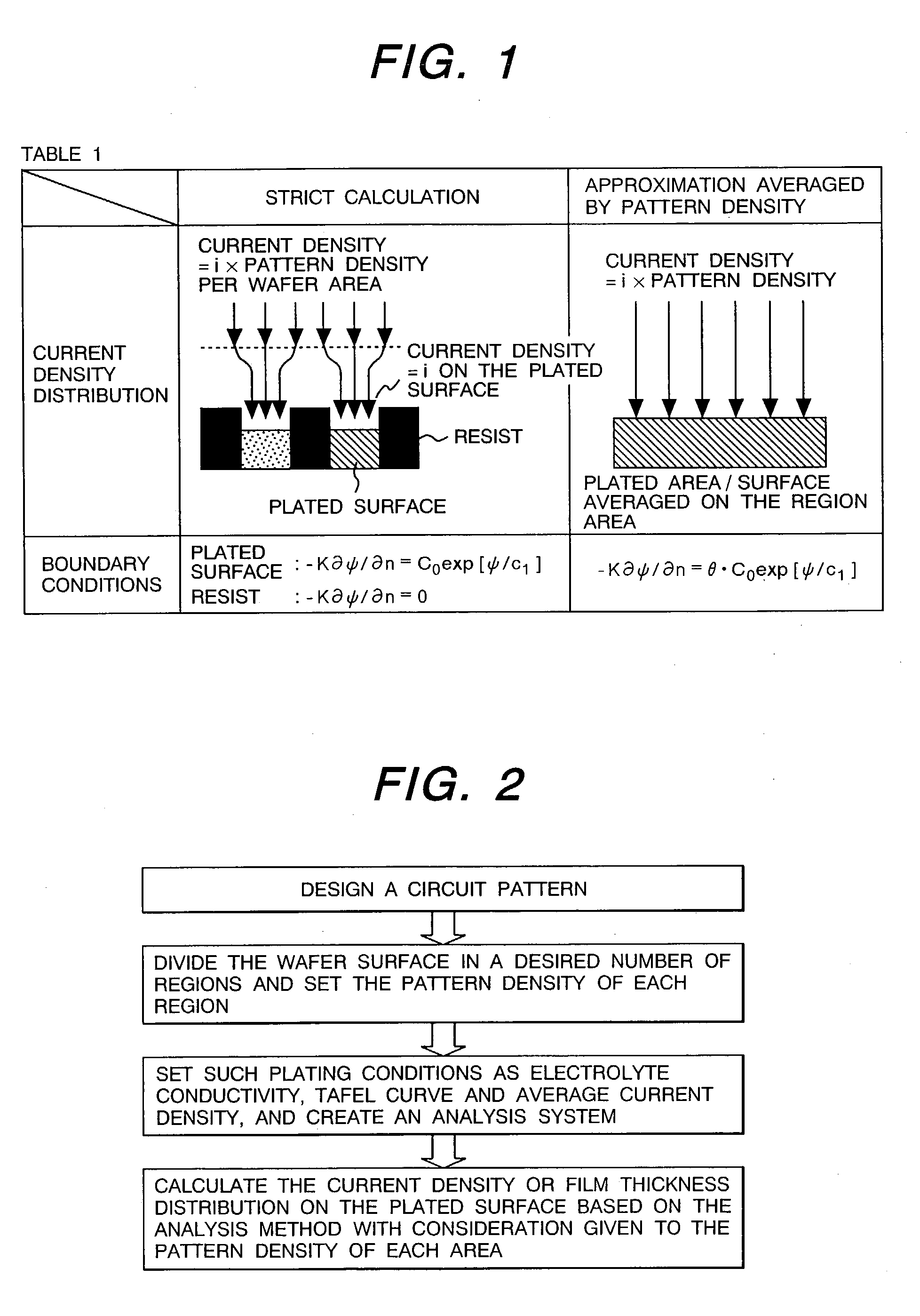
[0042] The following describes the present invention to explain that the approximation averaged by pattern density is also applicable to the analysis method where ion diffusion is taken into account.

[0043] A variety of ions are present in the electrolyte. The word "ion" appearing in the following description refers to the component for film formation in plating process. For example, it refers to Cu.sup.2+ion in the electrolyte in the electroplating for copper film formation.

[0044] The following describes the effect of ion diffusion. According to the equation (3) or (3b) where only the electric field effect is taken into account, the absolute value of current density .vertline.-K.differential..psi. / .differential.n.vertline. exhibits a more monotonous increase as the potential .psi. becomes greater. However, film forming speed is increased with current density. If there is an increase in film forming speed, ions in the vicinity of the plated surface are consumed by film formation on t...

first embodiment

[0047] Where .delta. denote the thickness of Nernst's diffusion layer, z charge of an ion, F a Faraday constant, D diffusivity of ion in electrolyte, and C.sub.bulk an ion concentration of bulk (a position removed from plated surface to electrolyte side by ".delta." or more). Other variables are the same as those used in the

[0048] In the equation (7) or (7b), the maximum value (.psi..fwdarw.infinite) is present to the current density. It is given by diffusion limited current=zFD C.sub.bulk / .delta.. In the region of current density sufficiently smaller than diffusion limited current, the equation is functional as in the case of equation (3) or (3b). Even when the effect of ion diffusion is taken into account, the concept of FIG. 1 (Table 1) of current density is valid and applicable; therefore, current density can be made uniform in the water area if current density is made so that it can be expressed by the following equation using the pattern density .theta.j of region j, as in the...

third embodiment

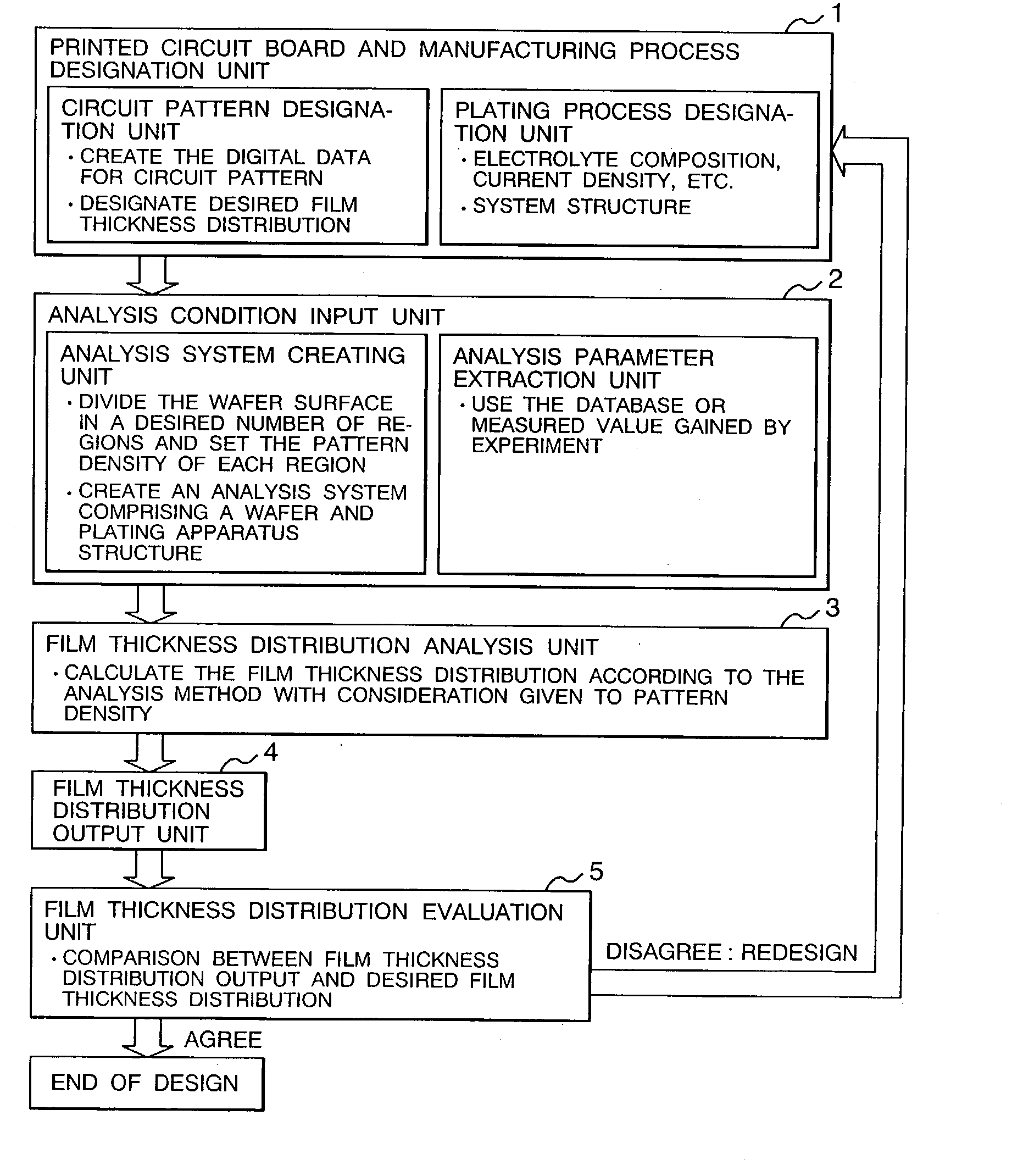
[0088] FIG. 7 is a figure representing a third embodiment according to the present invention. It shows a design system of printed circuit boards and manufacturing processes, based on the approximation averaged by pattern density according to the present invention.

[0089] In FIG. 7, a designation unit 1 for designating printed circuit boards and manufacturing process comprises a circuit pattern designation unit and plating process designation unit. The design system of the present embodiment mainly provides process designing in the step of plating in the circuit pattern designing and manufacturing process. The circuit pattern designation unit is designed in such a way that the circuit pattern permits electric operations that the printed circuit board is required to perform. For the sake of subsequent film thickness distribution analysis treatment, it is preferred that the circuit pattern be created in the form of digital data. Further, as shown in FIG. 7, information on desired film t...


PUM

PropertyMeasurementUnit
Thicknessaaaaaaaaaa
Current densityaaaaaaaaaa
Distributionaaaaaaaaaa

Abstract

The object of the present invention is to provide a film thickness distribution analysis method that ensures quick and effective prediction of film thickness distribution by computer simulation in the pattern plating process. On the circuit pattern of a printed circuit board, in the method for analyzing the thickness distribution of metal film plated selectively, hypothetically dividing the printed circuit board into one or more regions, introducing pattern density .theta.j=Aj/Sj (Sj: the area Sj of a desired region j, and Aj: the area of the plated surface inside the area j), and calculating the approximate average current density or film thickness distribution based on "approximation averaged by pattern density".

Description

BACKGROUND OF THE INVENTION[0001] 1. Field of the Invention[0002] The present invention relates to an analysis method of film thickness distribution and a design system of printed circuit boards and manufacturing processes in the process of using pattern plating method for forming a plated film on a circuit pattern on a selective basis where a printed circuit board is formed by electroplating.[0003] 2. Prior Art[0004] With recent increase in LSI speed and density, there has been a growing demand for lines of smaller size and greater number of multilayers in the printed circuit board for implementation of a semiconductor and mobile equipment.[0005] In the prior art, subtractive process has been widely employed to form lines on the printed circuit board. In the subtractive process, metal is formed (by panel plating) on the entire surface of the substrate by electroplating, and unwanted part of the line is removed by etching, whereby lines are formed on the printed circuit board. Howev...

Claims


Application Information

Patent Timeline
IPC IPC(8): C25D7/00C25D5/02G06F17/50H01L21/66H05K3/00H05K3/24
CPCG06F17/5009H05K3/241H05K3/0005G06F30/20H05K3/00
Inventor SANO, AKIHIROKOBAYASHI, KINYA
Owner HITACHI LTD
Why Eureka
Try Eureka