

Magnetically actuated microelectromechanical devices and method of manufacture
a technology of magnetic actuators and microelectromechanical devices, which is applied in the direction of mountings, optics, instruments, etc., can solve the problems of reducing the packing density of such arrays and higher insertion losses
- Summary
- Abstract
- Description
- Claims
- Application Information
AI Technical Summary
Benefits of technology
Problems solved by technology
Method used
Image

Examples
Embodiment Construction
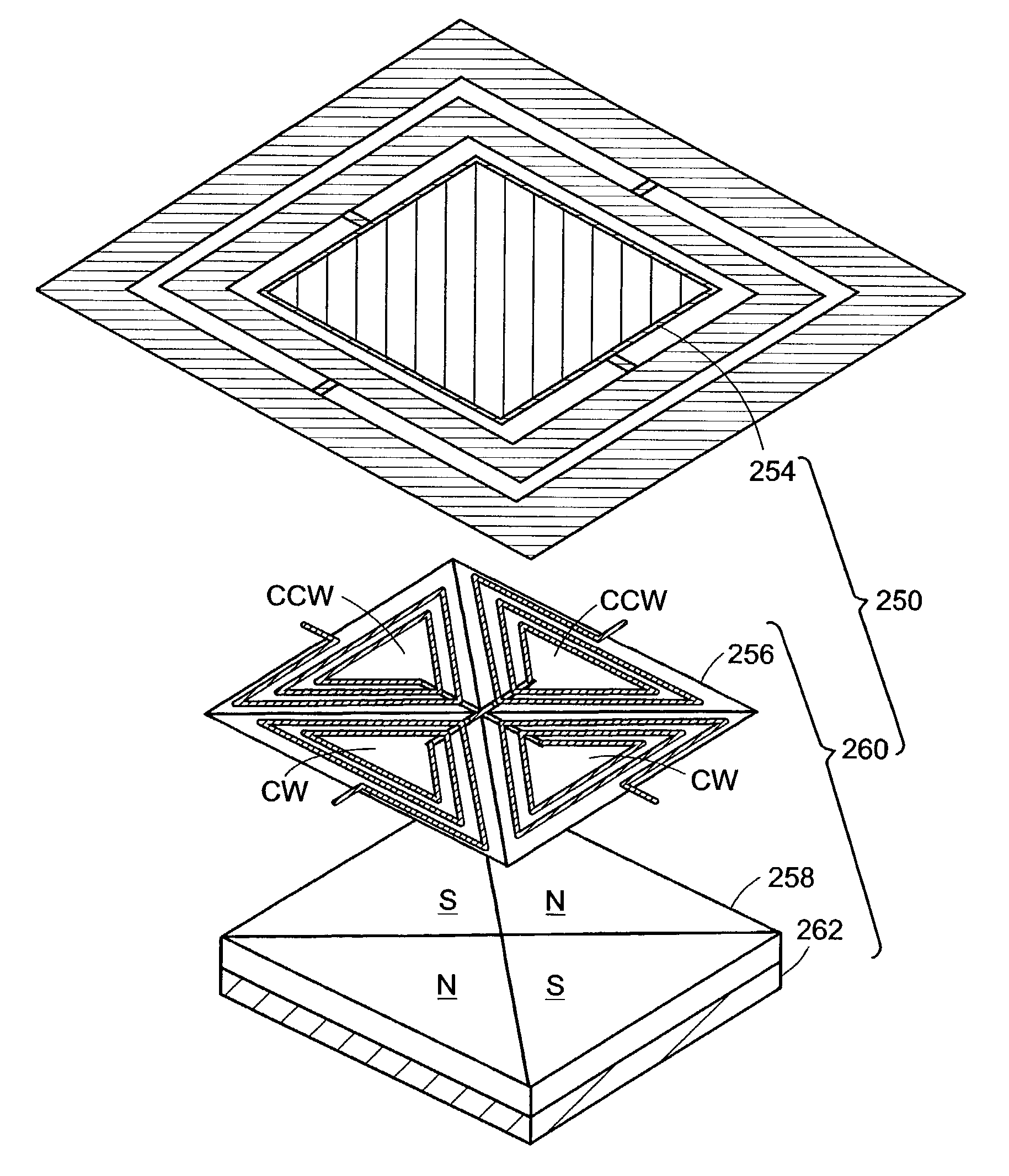
[0013] One embodiment of the invention is directed to a mirror device (for use in devices such as an optical switch, scanner or projector) having a movable mirror structure with an attached magnet. The mirror structure is movably mounted on a base structure, which includes an actuation coil for controlling movement of the mirror structure.
[0014] Another embodiment of the invention is directed to a mirror device (in a device such as an optical switch, scanner or projector) having a high mirror area fill factor. The device includes a mirror mounted on a support member, which is connected to a gimbal frame. The support member includes an enlarged portion configured to at least partially extend over the gimbal frame. The mirror substantially covers the enlarged portion of the support member, thereby providing the device with a high mirror area fill factor.
[0015] A further embodiment of the invention is directed to a mirror support structure for a movable mirror device (in a device such ...
PUM
 Abstract
Description
Claims
Application Information