Imaging device and manufacturing method for imaging device

a manufacturing method and imaging device technology, applied in the field of imaging devices, can solve the problems of miniaturizing the camera, and unable to shorten the length of the camera in an optical axis direction

Inactive Publication Date: 2003-10-30
FUJIFILM CORP +1
View PDF3 Cites 10 Cited by
  • Summary
  • Abstract
  • Description
  • Claims
  • Application Information

AI Technical Summary

Problems solved by technology

In the imaging device package described above, however, it is difficult to miniaturize a camera.
In any of these cases described above, however, the substrate or the base board for positioning is disposed in the rearward of the imaging device, so that it is impossible to shorten the length of the camera in an optical axis direction.
In other words, there is a disadvantage in miniaturizing the camera because the thickness of the camera cannot be slimed.
Therefore, there is a disadvantage that the imaging device results in increase in cost due to complex manufacturing process for actualizing the complex structure thereof.
The camera body becomes thin, because a base board and the like for fixing the imaging device chip on the substrate are unnecessary.

Method used


Image

  • Imaging device and manufacturing method for imaging device
  • Imaging device and manufacturing method for imaging device
  • Imaging device and manufacturing method for imaging device

Examples


first embodiment

[0046] (First Embodiment)

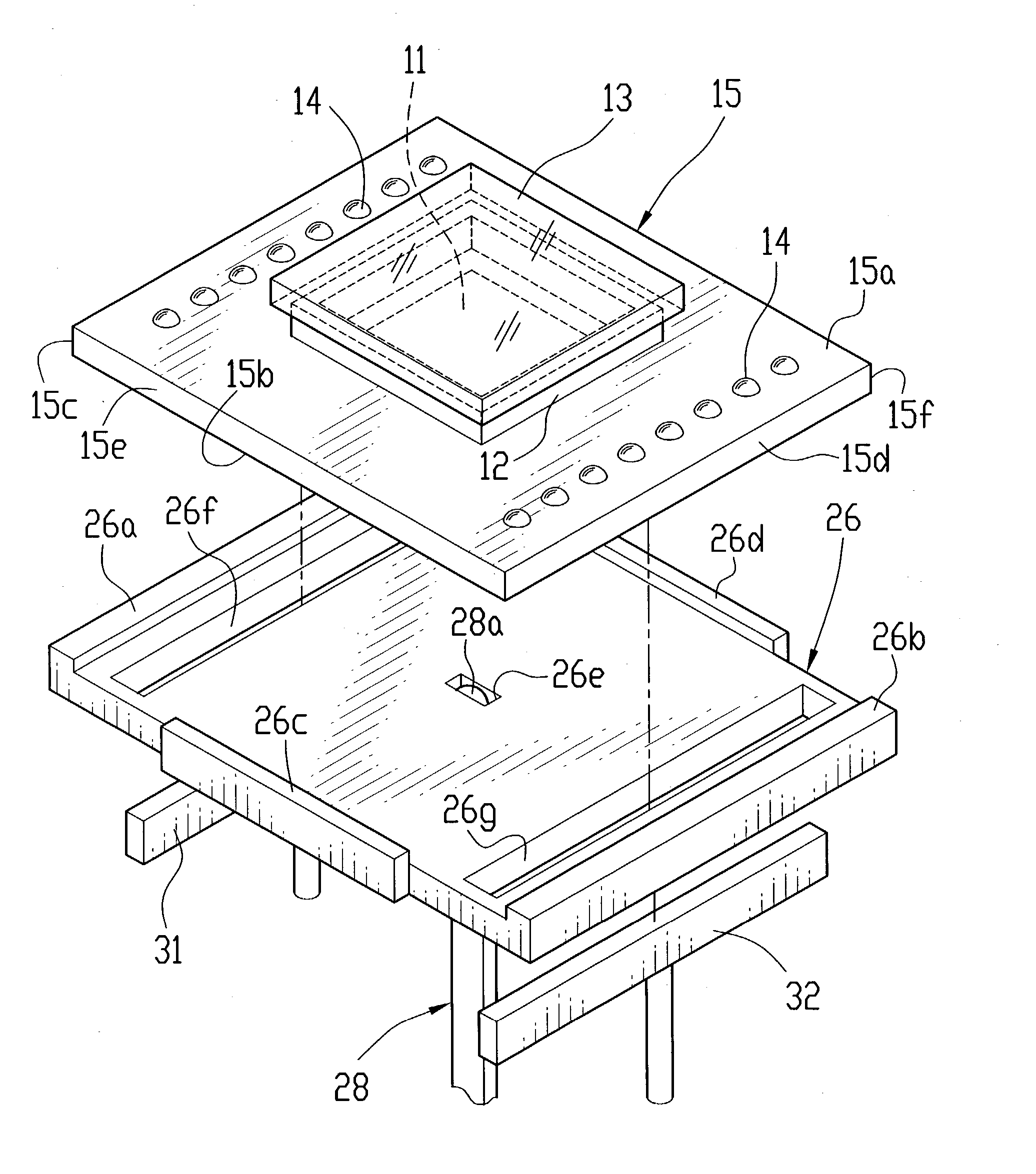
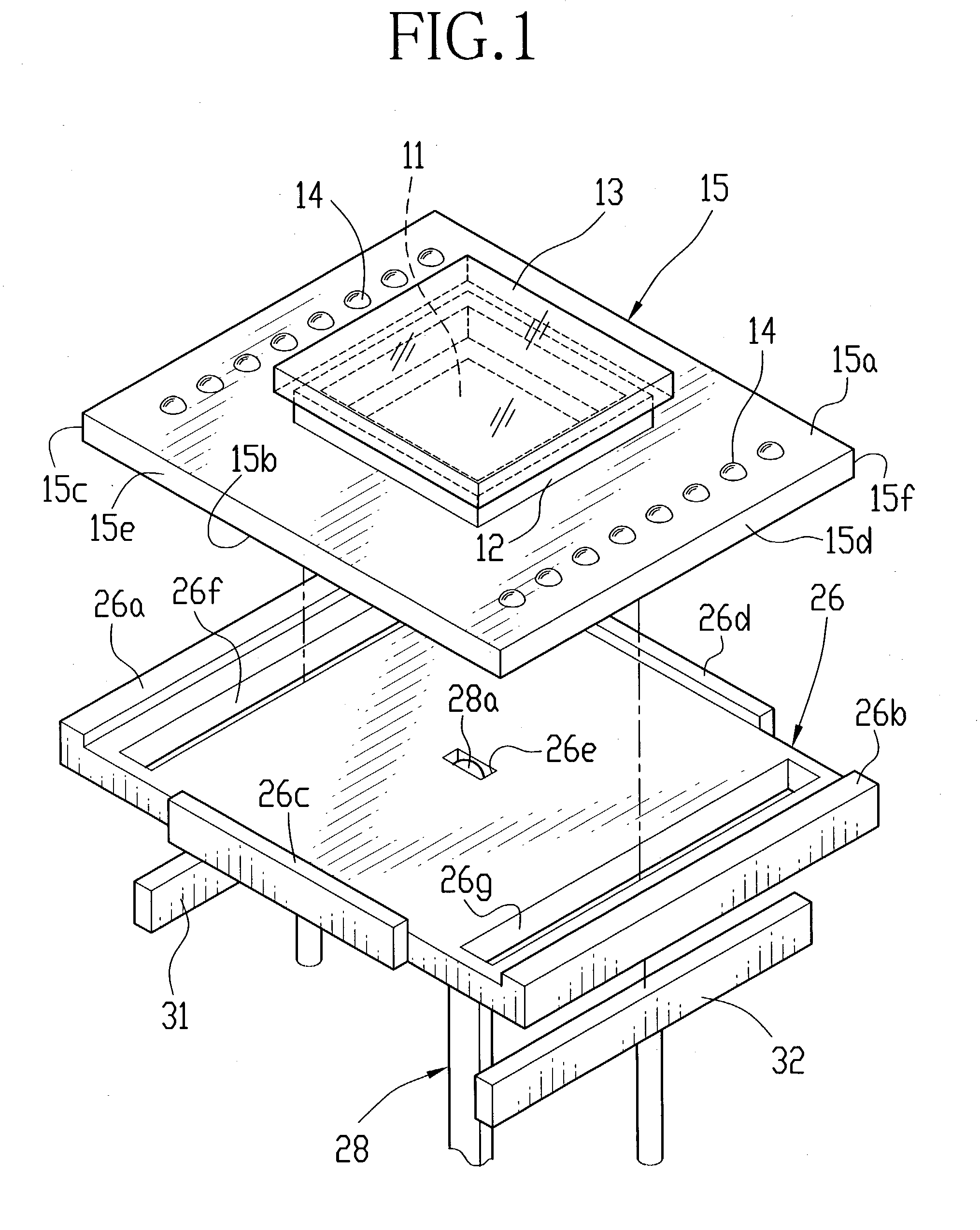
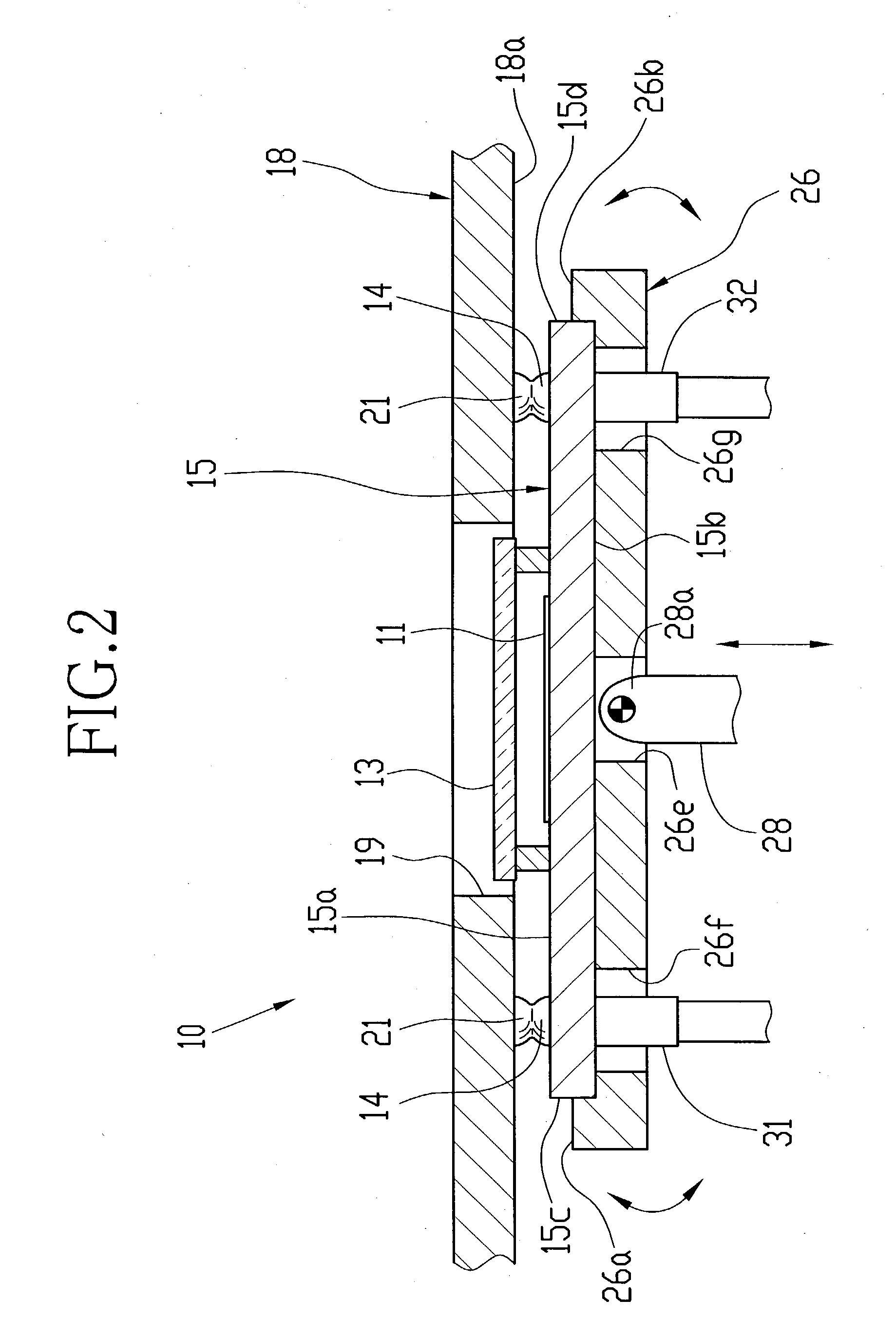
[0047] Referring to FIGS. 1 and 2, an imaging device 10 comprises a CCD (charge coupled device) chip 15 and a substrate 18 on which the CCD chip 15 is fixed. A light receiving surface 11 provided in the middle of the CCD chip is covered with a cover glass 13 via a frame shaped spacer 12. On the front surface 15a of the CCD chip 15, plural solder balls as chip terminals 14 are arranged in two lines. The lines of the chip terminals 14 are symmetrically disposed in parallel with each other across the light receiving surface 11.

[0048] An opening 19 is formed in the substrate 18. The cover glass 13 fits into the opening 19. On the rear surface 18a of the substrate 18, plural solder balls as substrate terminals 21 are arranged in two lines, which correspond to the lines of the chip terminals 14. Each of the substrate terminals 21 is soldered to the corresponding chip terminal 14. Various parts (not illustrated) for driving the CCD chip 15 are mounted on the substr...

second embodiment

[0058] (Second Embodiment)

[0059] Referring to FIGS. 4 and 5, an imaging device according to the second embodiment comprises the CCD chip 15 which is identical with that of the first embodiment, and a substrate 43 on which the CCD chip 15 is fixed. The substrate terminals 44 arranged on the substrate 43 are not solder balls as described in the first embodiment but plate shaped solder lands. The contact area of the chip terminal 14 with the solder land 44 is larger than that with the solder ball. Accordingly, the chip terminals 14 securely come into contact with the substrate terminals 44, so that a wide range of manufacturing error is allowable in comparison with a case of the solder balls.

[0060] A jig 40 is similar to that of the first embodiment in shape, but at least one pair of opposite protrusions 40a and 40b is higher than the thickness of the CCD chip 15. When the CCD chip 15 is mounted on the jig 40, the chip terminals 14 protrude from the protrusions 40a and 40b, because the...

third embodiment

[0063] (Third Embodiment)

[0064] FIG. 6 shows a CCD chip 47 composing an imaging device according to the third embodiment. Chip terminals 48 are so arranged on the front surface 47a of the CCD chip 47 as to surround a light receiving surface 49.

[0065] A T-shaped jig 45 the ends 45a to 45c of which bend perpendicularly is used for fixing the CCD chip 47 on a substrate. When the jig 45 moves in X and Y directions on a horizontal plane, the ends 45a to 45c make contact with the side surfaces 47c, 47d, and 47e of the CCD chip 47 respectively, in order to move the CCD chip 47 in the X and Y directions too. The substrate is provided with substrate terminals which correspond to the chip terminals 48. The CCD chip 47 is fixed on the substrate by the ultrasound or the partial heating, as in the case of the first or second embodiment.


PUM


Abstract

An imaging device unit comprises a CCD chip and a substrate on which the CCD chip is soldered. A light receiving surface is provided in the front surface of the CCD chip. A dustproof member for protect the light receiving surface from dust is attached around the light receiving surface. Chip terminals are arranged between the light receiving surface and the dustproof member. When the CCD chip is pressed against the rear surface of the substrate, the dustproof member is elastically deformed and tightly makes contact with the substrate. Since ultrasound is applied to the chip terminals and the substrate terminals in this state to melt them, the CCD chip is positioned in parallel with the substrate. Upon stopping ultrasound horns, both of the terminals are immediately soldered to each other, so that the CCD chip is securely fixed on the substrate with ease.

Description

[0001] 1. Field of the Invention[0002] The present invention relates to an imaging device which contributes to the reduced thickness of a camera.[0003] 2. Background Arts[0004] A digital camera and a video camera, which rapidly become pervasive in recent years, are provided with an imaging device chip such as a CCD image sensor, a CMOS image sensor, and the like. The imaging device chip photoelectrically transfers an image which is optically formed on a light receiving surface into image signals. The outputted image signals are sent to an image signal processing circuit, for example, and the image is displayed on an LCD. To obtain the sharp image over the whole picture frame, it is necessary to install the imaging device chip in such a manner that the light receiving surface is perpendicular to an optical axis. Accordingly, various types of imaging devices are suggested.[0005] Japanese Patent Laid-Open Publication No. 61-138909, for example, discloses a solid-state image sensor unit...

Claims


Application Information

Patent Timeline
Patent Type & Authority Applications(United States)
IPC IPC(8): H04N5/225H01L27/14H04N5/335
CPCH04N5/2253H04N2007/145H04N5/2254H01L27/14618H01L27/14625H04N23/52H04N23/54H04N23/55
Inventor MISAWA, ATSUSHI
Owner FUJIFILM CORP
Why Eureka
Try Eureka