Fabrication method of a three-dimensional microstructure

a technology of three-dimensional microstructure and fabrication method, which is applied in the direction of photomechanical equipment, instruments, photosensitive material processing, etc., can solve the problems of microstructure damage, metal mask 24 is a thin film liable to crack thereon, and the problem of adhesion uniformity between them is a serious concern

Inactive Publication Date: 2003-11-20
NATIONAL TSING HUA UNIVERSITY
View PDF5 Cites 8 Cited by
  • Summary
  • Abstract
  • Description
  • Claims
  • Application Information

AI Technical Summary

Problems solved by technology

However, this method must apply many different materials to finish one layer of embedded channel.
Unfortunately, the metal mask 24 is a thin film liable to have cracks thereon.
Furthermore, the microstructure is also caused damage by the removal of the metal mask 24 thereafter.
The adhesion unif...

Method used


Image

  • Fabrication method of a three-dimensional microstructure
  • Fabrication method of a three-dimensional microstructure
  • Fabrication method of a three-dimensional microstructure

Examples


Embodiment Construction

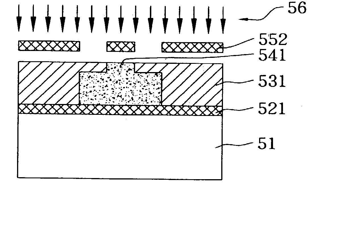
[0022] FIGS. 5(a)-5(f) show diagrams of the fabrication process of a 3D microstructure in accordance with the present invention. A substrate 51 is uniformly coated with a first anti-reflection layer 521, as shown in FIG. 5(a). We can use a semiconductor wafer as the substrate 51. The first anti-reflection layer 521 is a photoresist capable of absorbing reflected light on the resist-substrate interface. The CK-6020L resist made by Fujifilm Co. is suitable to be used as a material for the anti-reflection layer due to its properties. In particular, UV light is completely absorbed by the CK-6020L resist.

[0023] The first anti-reflection layer 521 is overlaid with a first SU-8 layer by a spin-on method. After the first exposure step by a first photo mask 551, the SU-8 layer is defined as exposed areas 531 and unexposed areas 541, as shown in FIG. 5(b). SU-8, a thick negative photoresist, has been used in the fabrication of microstructures for several years, because it has a high aspect ra...


PUM


Abstract

A fabrication method of three-dimensional microstructures is to fabricate a real 3D microstructure. First, a substrate is coated with an anti-reflection layer to absorb reflected exposure light, and then the anti-reflection layer is overlaid with a first thick photoresist. After having been fully exposed by a first photo mask, a predetermined exposure depth of the first thick photoresist is achieved by a second photo mask and dosage-controlled UV exposure. If the unexposed areas of the first thick photoresist are released during a development step, a single-layer microstructure is created. Inversely, a multi-layered microstructure can be obtained simply by repeating the process described above. After all layers are laminated on the substrate, all unexposed areas of the all thick photoresist layers are released and connected to each other during a development step.

Description

[0001] 1. Field of the Invention[0002] The present invention relates to a fabrication method of three-dimensional (3D) microstructure, and more particularly, to a semiconductor process employing a thick photoresist by controlling exposure dosage to form a microstructure on a substrate.[0003] 2. Description of the Related Art[0004] In recent years, microstructure devices have been developed for biochemistry, sensor science and pharmaceutics, and also have given rise to the advent of various fabrication techniques to fabricate microstructures made from various materials.[0005] Embedded micro channels are generally used for microstructure devices to distribute and store micro fluid, and find applications in areas such as reagents, pharmaceuticals or inkjet printheads. There are at least four major methods that have been reported that use thick photoresist, such as SU-8 resist, to fabricate embedded micro channel structures. All the methods are superior to other non-mentioned micromachi...

Claims


Application Information

Patent Timeline
IPC IPC(8): G03F7/00G03F7/20H01L21/027
CPCG03F7/0035G03F7/0037G03F7/203Y10S430/151G03F7/70416H01L21/0276G03F7/7035B81C1/00G03F7/20
Inventor TSENG, FAN-GANGCHUANG, YUN-JU
Owner NATIONAL TSING HUA UNIVERSITY
Why Eureka
Try Eureka