Optical waveguide structures

a waveguide and optical technology, applied in the field of optical devices, can solve the problems of limited practical interest for lossy plasmon-polariton waves guided by metal-dielectric interfaces, and infinitely wide metal film structures

Inactive Publication Date: 2004-01-15
UNIVERSITY OF OTTAWA
View PDF13 Cites 57 Cited by
  • Summary
  • Abstract
  • Description
  • Claims
  • Application Information

AI Technical Summary

Problems solved by technology

Infinitely wide metal film structures, however, are of limited practical interest since they offer one-dimensional (1-D) field confinement only, with confinement occurring along the vertical axis perpendicular to the direction of wave propagation, implying that modes will spread out laterally as they propagate from a point source used as the excitation.
In addition to the lack of lateral confinement, plasmon-polariton waves guided by a metal-dielectric interface are in general quite lossy.
Even long-range surface plasmons guided by a metal film can be lossy by comparison with dielectric waveguides.
This results in a modulation in the intensity of the light exiting the dielectric waveguide.
These known modulation and switching devices disadvantageously require relative high control voltages and have limited electrical/optical bandwidth.
The use of numerical methods to solve differential equations inevitably raises questions regarding the co

Method used


Image

  • Optical waveguide structures
  • Optical waveguide structures
  • Optical waveguide structures

Examples


Embodiment Construction

OF APPLICATION

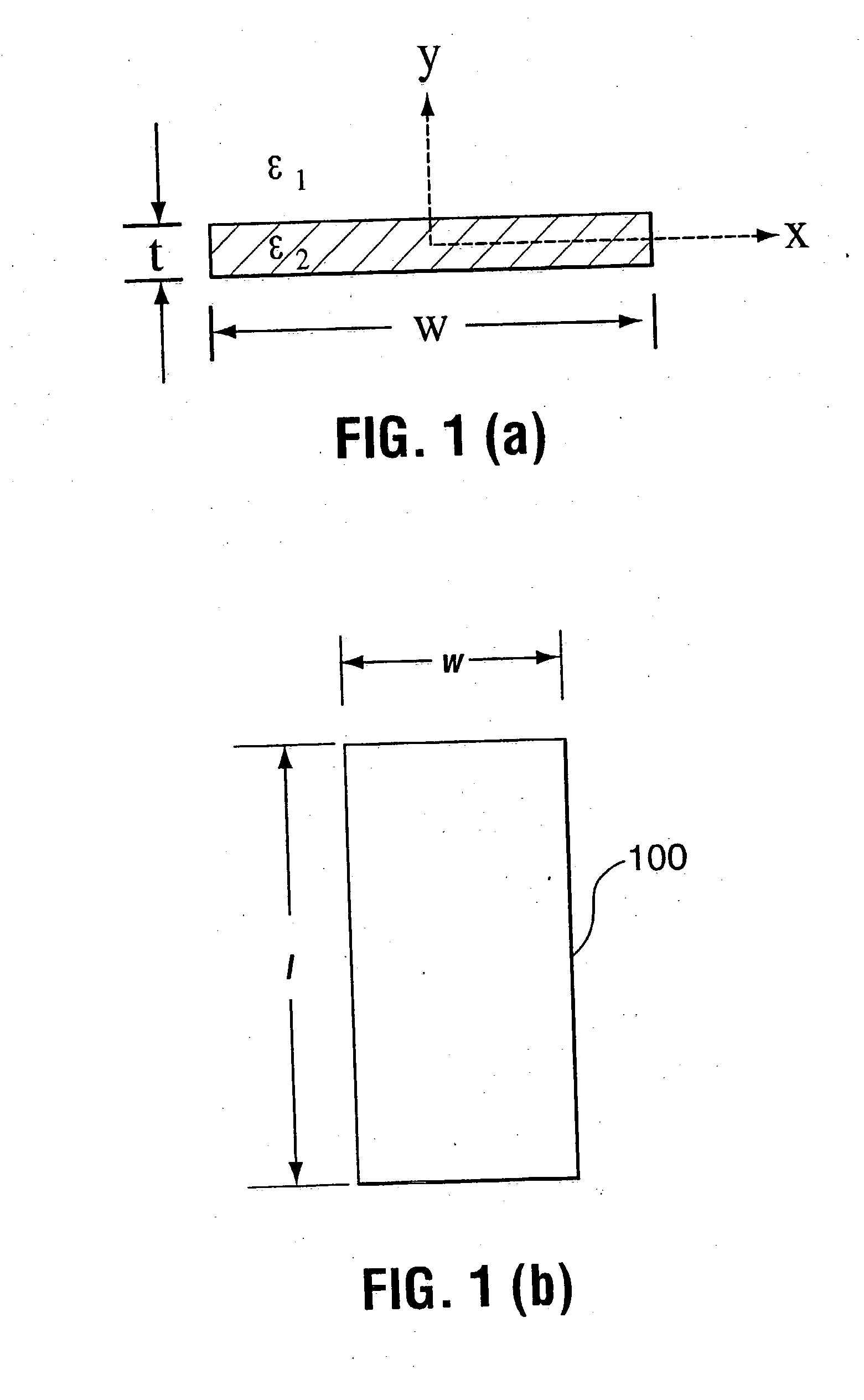
[0221] Examples of practical waveguide structures, and integrated optics devices which can be implemented using the invention, will now be described with reference also to FIGS. 27 to 42, 51 and 52. Unless otherwise stated, where a waveguide structure is shown, it will have a general construction similar to that shown in FIGS. 1(a) and 1(b) or that shown in FIGS. 17(a) and 17(b).

[0222] Waveguides, structures and devices disclosed herein operate with radiation:

[0223] having a wavelength such that a plasmon-polariton wave is supported;

[0224] at optical wavelengths;

[0225] at optical communications wavelengths;

[0226] at wavelengths in the range of 800 nm to 2 .mu.m;

[0227] at wavelengths near 1550 nm;

[0228] at wavelengths near 1310 nm;

[0229] at wavelengths near 850 nm;

[0230] at wavelengths near 980 nm.

[0231] It should be appreciated that references to wavelength should be interpreted as meaning the centre free space wavelength of the spectrum associated with the input radia...


PUM


Abstract

The purely bound electromagnetic modes of propagation supported by waveguide structures comprised of a thin lossy metal film of finite width embedded in an infinite homogeneous dielectric have been characterized at optical wavelengths. One of the fundamental modes supported by the structure exhibits very interesting characteristics and is potentially quite useful. It evolves with decreasing film thickness and width towards the TEM wave supported by the background (an evolution similar to that exhibited by the sb mode in symmetric metal film slab waveguides), its losses and phase constant tending asymptotically towards those of the TEM wave. Attenuation values can be well below those of the sb mode supported by the corresponding metal film slab waveguide. Low mode power attenuation in the neighbourhood of 10 to 0.1 dB/cm is achievable at optical communications wavelengths, with even lower values being possible. Carefully selecting the film's thickness and width can make this mode the only long-ranging one supported. In addition, the mode can have a field distribution that renders it excitable using an end-fire approach. The existence of this mode renders the finite-width metal film waveguide attractive for applications requiring short propagation distances and 2-D field confinement in the transverse plane, enabling various devices to be constructed, such as couplers, splitters, modulators, interferometers, switches and periodic structures. Under certain conditions, an asymmetric structure can support a long-ranging mode having a field distribution that is suitable to excitation using an end-fire technique. Like asymmetric slab waveguides. The attenuation of the long-ranging mode near cutoff decreases very rapidly, much more so than the attenuation related to the long-ranging mode in a similar symmetric structure. The cutoff thickness of a long-ranging mode in an asymmetric finite-width structure is larger than the cutoff thickness of the sb mode in a similar asymmetric slab waveguide. This implies that the long-ranging mode supported by an asymmetric finite-width structure is more sensitive to the asymmetry in the structure compared to the sb mode supported by a similar slab waveguide. This result is interesting and potentially useful in that the propagation of such a mode can be affected by a smaller change in the dielectric constant of the substrate or superstrate compared with similar slab structures.

Description

[0001] This is a Continuation-in-Part of U.S. patent application Ser. No. 09 / 742,422 which itself was a Continuation-in-Part of U.S. patent application Ser. No. 09 / 629,816 filed Jul. 31, 2000, now U.S. Pat. No. 6,442,321 issued Aug. 27, 2002, and which claimed priority from U.S. Provisional patent application No. 60 / 171,606 filed Dec. 23, 1999, Canadian patent application No. 2,314,723 filed Jul. 31, 2000 and Canadian patent application No. 2,319,949 filed Sep. 20, 2000. The contents of these applications are incorporated herein by reference.[0002] 1. Technical Field[0003] The invention relates to optical devices and is especially applicable to waveguide structures and integrated optics.[0004] 2. Background Art[0005] This specification refers to several published articles. For convenience, the articles are cited in full in a numbered list at the end of the description and cited by number in the specification itself. The contents of these articles are incorporated herein by reference...

Claims


Application Information

Patent Timeline
IPC IPC(8): G02B6/12G02B6/122G02B6/125G02F1/19G02F1/225G02F1/313
CPCB82Y20/00G02B6/122G02B6/1225G02B6/125G02B2006/12145G02F2203/10G02B2006/1215G02B2006/12159G02F1/195G02F1/225G02F1/3132G02B2006/12147
Inventor BERINI, PIERRE SIMON JOSEPH
Owner UNIVERSITY OF OTTAWA
Why Eureka
Try Eureka