Technique for microstructuring replication mold

a micro-structuring and mold technology, applied in the field of micro-structuring replication molds, can solve the problems of limited microstructures, complicated basic form fabrication process, and inability to produce very fine micro- or nano-structures

Inactive Publication Date: 2004-02-19
CSEM CENT SUISSE DELECTRONIQUE & DE MICROTECHNIQUE SA RECH & DEV
View PDF10 Cites 38 Cited by
  • Summary
  • Abstract
  • Description
  • Claims
  • Application Information

AI Technical Summary

Problems solved by technology

Conventional techniques such as direct machining are not capable of producing very fine micro- or nano-structures such as required for antireflection grating surfaces.
The fabrication of an original form with such grating microstructure is possible, but complicates the basic form fabrication process.
This approach is limited to microstructures in the order of micrometers in relief amplitude and is not suitable for fabricating deeper refractive lenses with relief amplitudes in the order of mm.
It is also limited to relatively shallow (micrometer relief) microstructures together with materials such as quartz which can be patterned lithographically and is not suitable for the preferred metal tool inserts.
The approach described is limited to circularly symmetric microstructures and is not suitable for fabricating submicrometer squarewave grating profiles.

Method used


Image

  • Technique for microstructuring replication mold
  • Technique for microstructuring replication mold
  • Technique for microstructuring replication mold

Examples


Embodiment Construction

[0019] Embodiments of the invention will now be described by way of example, with reference to the drawings, in which:

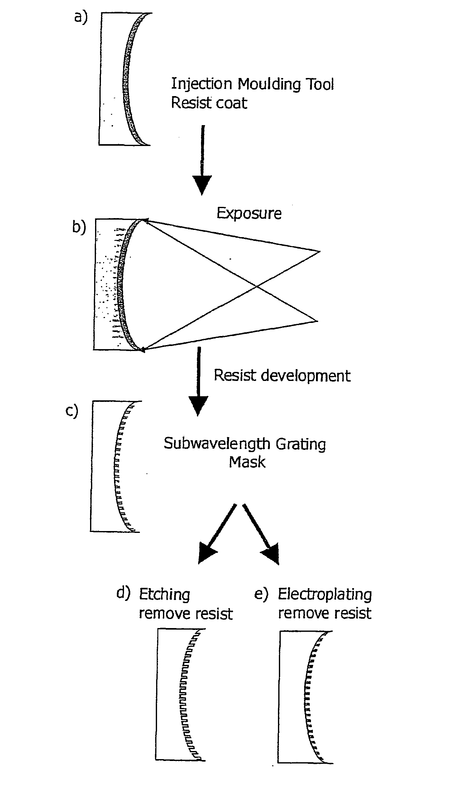
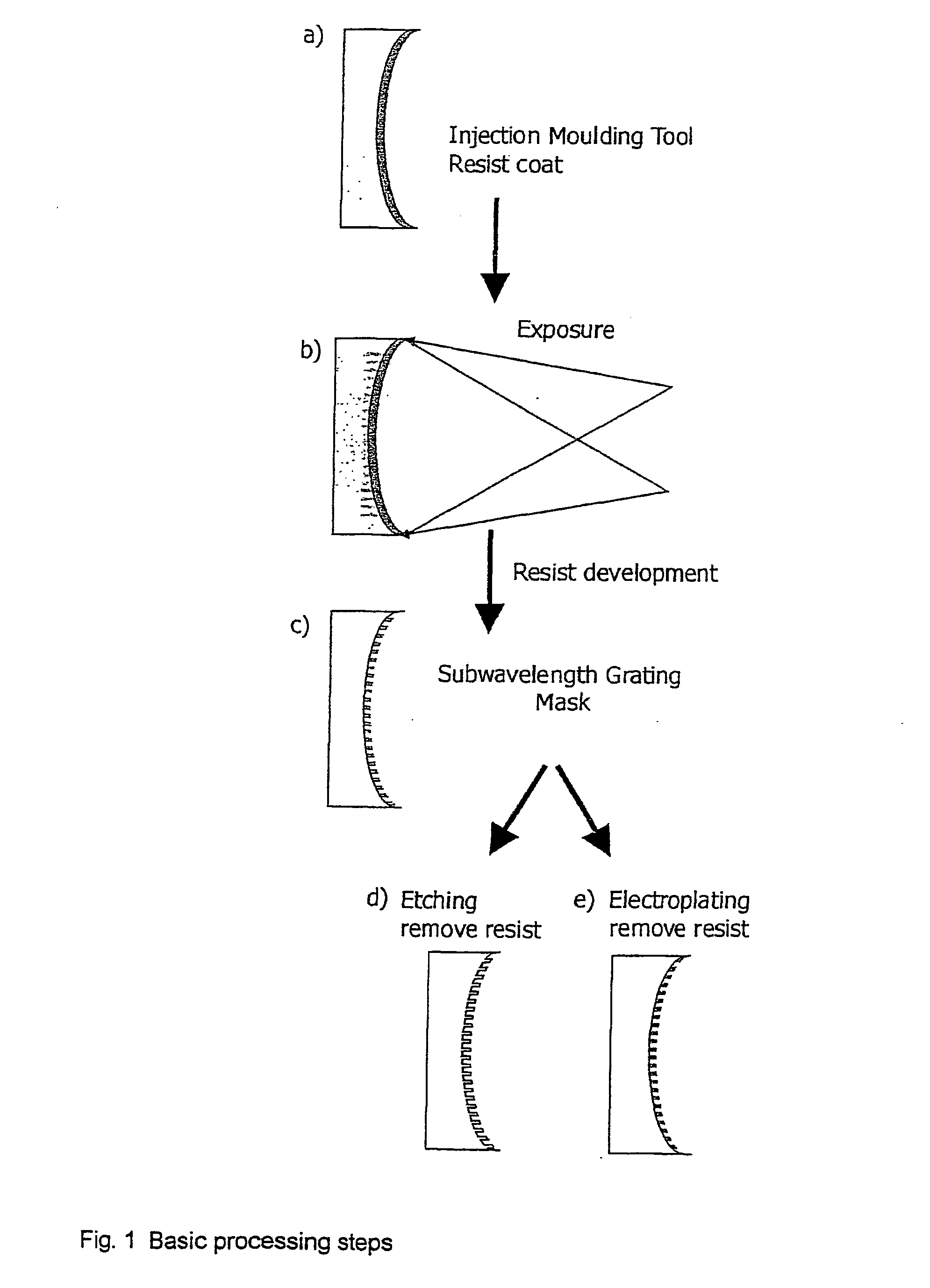
[0020] FIG. 1 illustrates the processing steps of a method embodying the invention; and

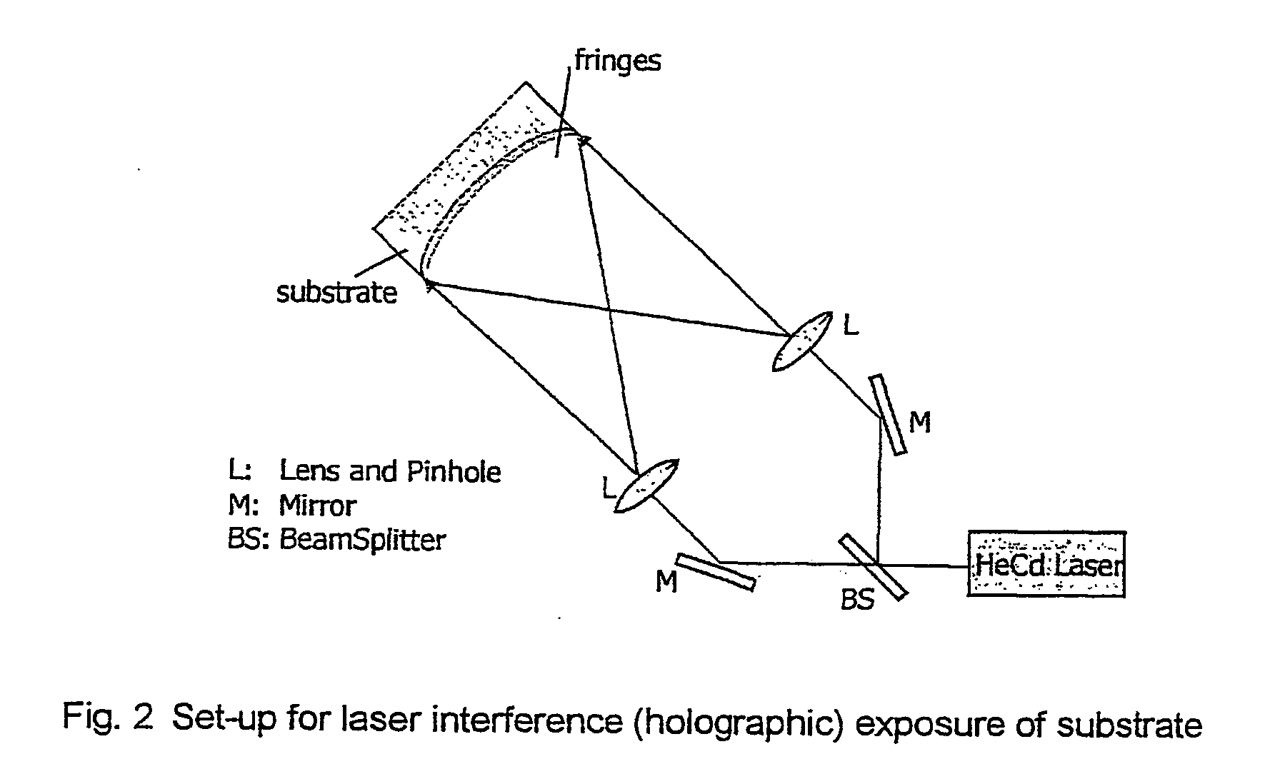
[0021] FIG. 2 illustrates the holographic exposure of a substrate of a curved mould surface.

[0022] FIG. 1 illustrates the technique for the fabrication of a high resolution, subwavelength AR (Anti-reflection) grating microstructure. Such gratings have the following typical parameters:

[0023] Periodicity: 200-400 nm

[0024] Linewidths: 100-200 nm

[0025] Relief depth: 100-200 nm

[0026] The details of the processing steps (c.f. FIG. 1) are as follows:

[0027] 1. Mask Fabrication

[0028] (a) The mould insert is coated with a thin film of photoresist (such as Shipley 1800 series). The coating of uniform thickness films on non-planar surfaces is difficult and requires special coating technology. An alternative to commercial photoresists are developmental systems such as dry resists of the chalcog...


PUM

PropertyMeasurementUnit
depthsaaaaaaaaaa
Relief depthaaaaaaaaaa
depthaaaaaaaaaa

Abstract

A surface microstructure is superimposed on the surface of a replication mould such as an injection moulding tool insert by laser interference exposure of a mask pattern and etching or electroplating the additional microstructure. The technique enables the post-processing of planar and non-planar replication moulds with additional microstructure to improve the functionality and value of the moulded components. A major area of application is an anti-reflection surface for injection moulded polymer optical components, achieved by the superposition of submicrometer anti-reflection grating structure onto injection moulding tool inserts.

Description

[0001] This invention relates to the production of moulded polymer components, for example, by injection moulding, hot embossing, UV-embossing or other replication technologies. Examples of such components include optical elements such as lenses and optical microsystems composed of multiple elements. Applications are primarily in optical systems for sensors, instruments, telecommunications and displays.PRIOR ART[0002] Replication technology such as injection moulding is an important fabrication technology for optical elements and Microsystems. A summary of replication technology for optical elements can be found in (1). The technology for fabrication of moulds directly or from an original form is well established. Major approaches are the direct fabrication of the mould insert in metal by high precision machining or diamond turning, and the electroforming of a Ni shim or mould insert from an original form.[0003] The use of very fine surface structures with micrometer or submicromete...

Claims


Application Information

Patent Timeline
Patent Type & Authority Applications(United States)
IPC IPC(8): B29C33/38B29C33/42B29C45/37G02B5/18G03H1/04
CPCB29C33/3842B29C33/424B29C45/372B29L2011/0016G02B5/008G03H2260/63G03H1/04G03H2001/0284G03H2001/043G03H2260/14G02B5/1866
Inventor GALE, MICHAELSOCHTIG, JUERGENROSSI, MARKUS
Owner CSEM CENT SUISSE DELECTRONIQUE & DE MICROTECHNIQUE SA RECH & DEV
Why Eureka
Try Eureka