Adjustment in a MAPPER system

a mapper and adjustment technology, applied in the field of lithography systems, can solve the problems of affecting affecting the accuracy of the alignment, and putting a heavy burden on the alignment of the different parts of the system,

Inactive Publication Date: 2004-03-18
ASML NETHERLANDS BV
View PDF3 Cites 31 Cited by
  • Summary
  • Abstract
  • Description
  • Claims
  • Application Information

AI Technical Summary

Problems solved by technology

Due to the fact that these systems are all optical, the resolution is diffraction limited.
A problem, which thus emerges in a MAPPER system, is that the extra components compared to known deep-UV lithographic systems were found to put a heavy burden on alignment of the different parts of the system.
Furthermore, it was found that even with perfect alignment of the MAPPER system, because of tolerances between converter plates, the alignment after replacement of parts and / or of a mask would not be as perfect as it was at first.
Even worse, the system would not be able to cope with slight expansion or contraction of wafers between process steps, for which the magnification between mask and wafer must be adjusted.
However, it can be easily understood that even without a mask the alignment of all other components remains extremely difficult.

Method used


Image

  • Adjustment in a MAPPER system
  • Adjustment in a MAPPER system
  • Adjustment in a MAPPER system

Examples


first embodiment

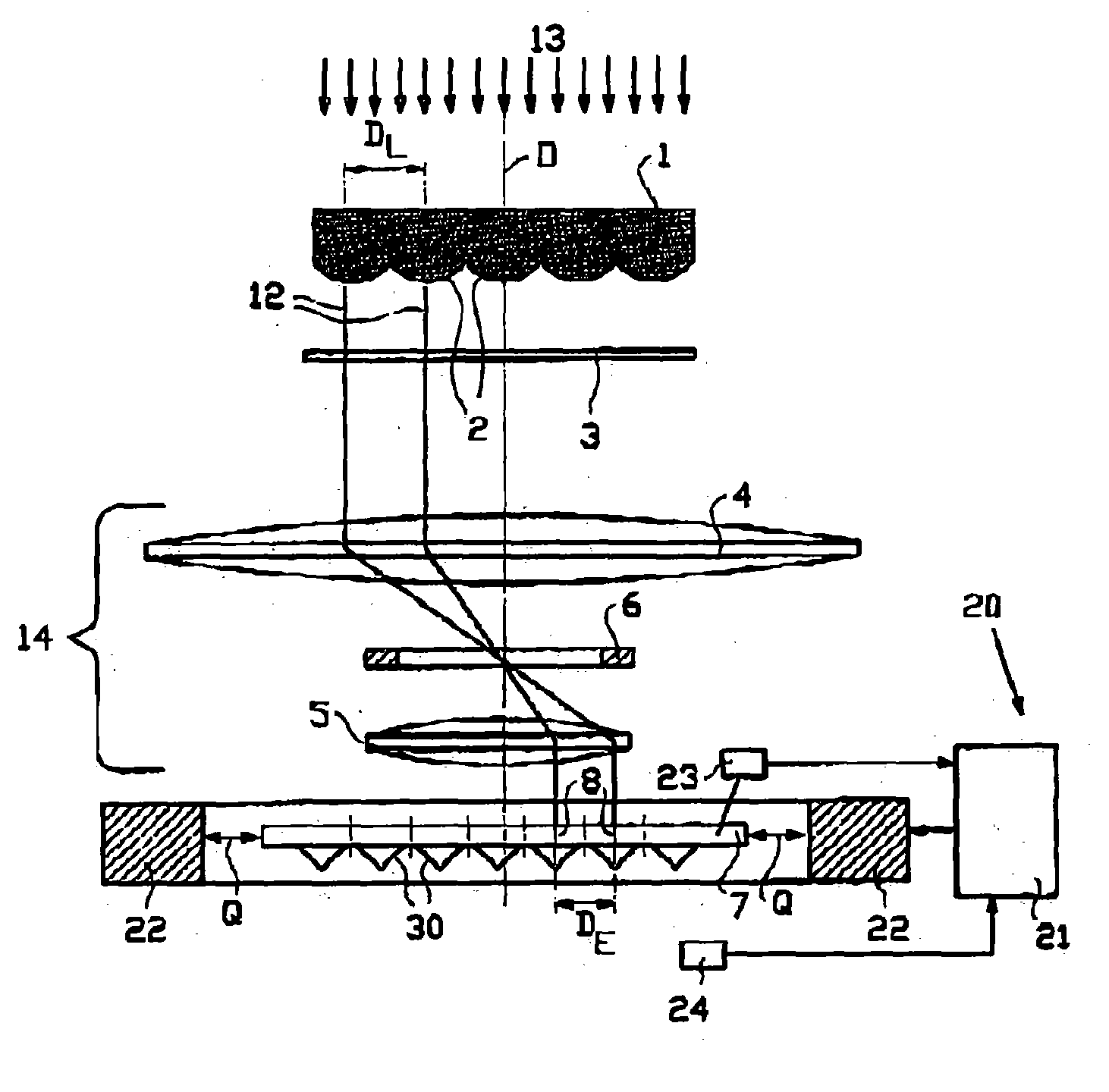
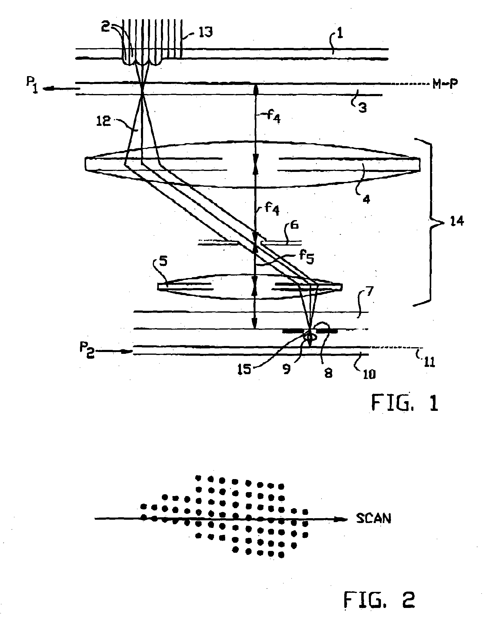
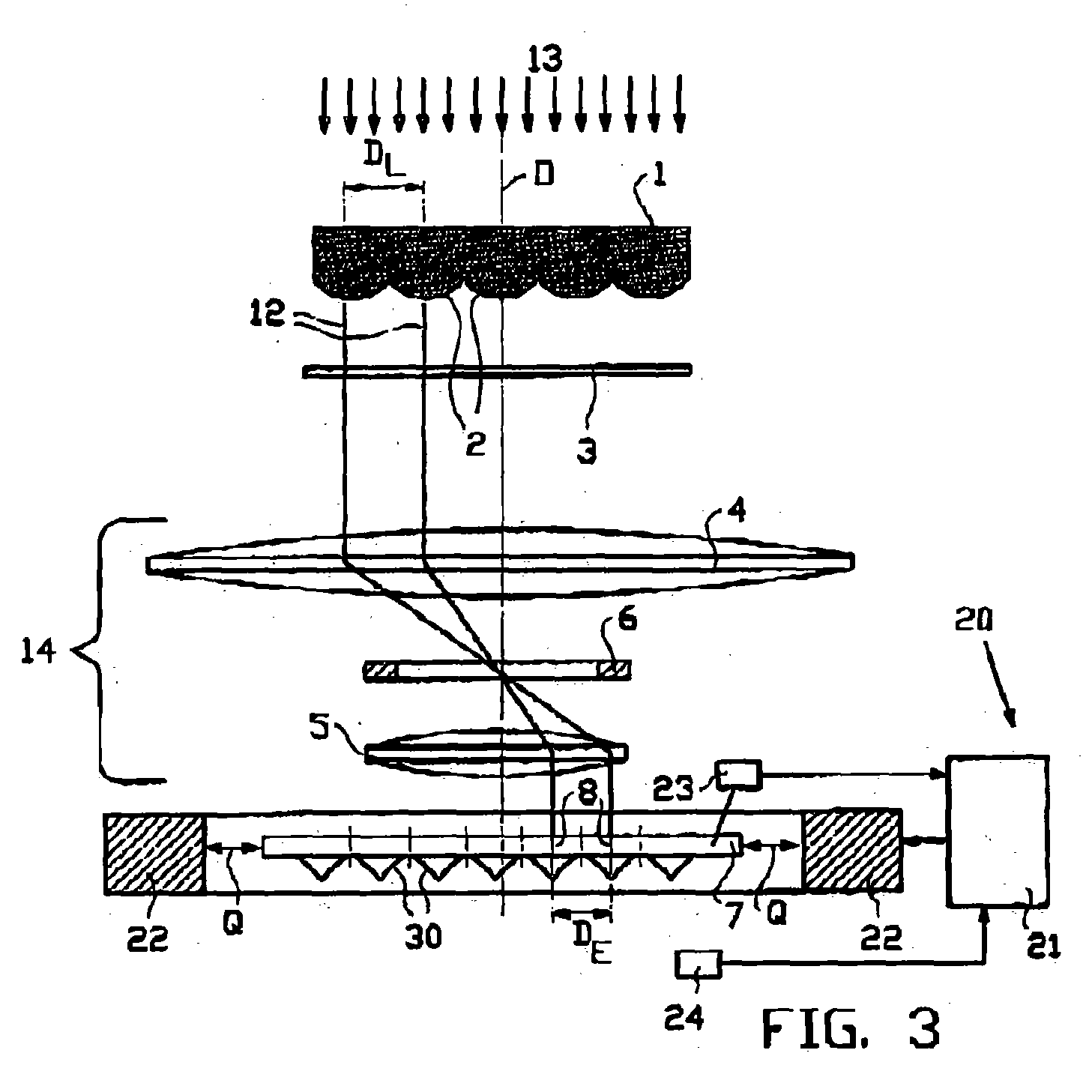
[0086] FIG. 3 shows schematically a lithography system according to the present invention, which uses a fine adjustment of the converter by converter-related thermal means. In the converter plate 7, as described in PCT / NL00 / 00657, semiconductor field emitter tips 30 are used as converter elements 8. The adjacent field emitter tips 30 are spaced apart at an element distance D.sub.E, which indicates the intermediate distance between the respective centres of the adjacent converter elements 8. In the micro lens array 1 adjacent lenses 2 are located at an intermediate lens distance D.sub.L, which denotes the distance between the optical axes 26 of adjacent lenses 2.

[0087] The projection of each light beamlet 12 from a respective lens 2 in the micro lens array 1 on the converter plate 7 should largely coincide with a converter element 8. The demagnifying optics 14 must match the lens distance D.sub.L of adjacent lenses 2 in the micro lens array 1 to the element distance D.sub.E of adjace...

third embodiment

[0103] In FIG. 5 the present invention is shown. In this embodiment, the thermal means change the temperature of a mask when present in the lithography system. The system is further equal to the system of FIGS. 3 and 4.

[0104] In a second main embodiment, various specific embodiments of which are shown if FIGS. 6-8, the control means comprise mechanical means for applying mechanical forces to various parts of the system. By applying mechanical forces, it also showed possible to adjust the physical dimensions of various main components of a MAPPER system. Again, identical reference numerals show identical components.

[0105] The basic layout of the embodiments shown in FIGS. 6-8 is identical. A detector 24 measures the deviation of a specific main component, like the micro lens array, the mask or the converter. A controller 21 compares the measured values with the desired values. The controller further comprises, in its memory, information regarding the response of that specific main co...


PUM

PropertyMeasurementUnit
diameteraaaaaaaaaa
spot sizeaaaaaaaaaa
spot sizeaaaaaaaaaa

Abstract

The present invention relates to a lithography system comprising: means for generating a plurality of light beamlets, and an electron source, arranged to be illuminated by said light beamlets, said electron source comprising a plurality of converter elements at an element distance from each other for converting a light beamlet impinging onto it into an electron beamlet directed towards and focussed on an object plane, said lithography system further comprising control means for manipulating the mutual positions of the light beamlets with respect to the converter elements. These control means can be of optical, thermal, mechanical or magnetical nature, and work on for instance the micro lens array, the converter plate, and the mask.

Description

[0001] The present invention relates to a lithography system comprising:[0002] means for generating a plurality of light beamlets, and[0003] an electron source, arranged to be illuminated by said light beamlets, said electron source comprising a plurality of converter elements at an element distance from each other for converting a light beamlet impinging onto it into an electron beamlet directed towards and focussed on an object plane.PRIOR ART[0004] Current lithography systems are mostly all optical, deep UV systems. These systems use light in the deep UV region, i.e. up to 193 nm. Due to the fact that these systems are all optical, the resolution is diffraction limited. The resolution of these systems is about 130 nm at present.[0005] WO 98 / 54620, which is incorporated herein by reference as it fully set forth, discloses a lithography system, which will be described with reference to FIGS. 1 and 2.[0006] In the lithography system, a light source (not shown) produces a light beam ...

Claims


Application Information

Patent Timeline
Patent Type & Authority Applications(United States)
IPC IPC(8): G03F7/20
CPCB82Y40/00G03F7/2051G03F7/2059H01J37/065B82Y10/00H01J37/3174H01J2237/06333H01J2237/24514H01J37/073
Inventor KRUIT, PIETER
Owner ASML NETHERLANDS BV
Why Eureka
Try Eureka