Method of etching variable depth features in a crystalline substrate

a technology of variable depth and crystalline substrate, which is applied in the direction of microstructural devices, coatings, microstructured devices, etc., can solve the problems of affecting analytical results, deviation from the calculated channel volume, and the miniaturization of interconnecting channels such as small

Inactive Publication Date: 2004-03-18
APPLIED MATERIALS INC
View PDF19 Cites 15 Cited by
  • Summary
  • Abstract
  • Description
  • Claims
  • Application Information

AI Technical Summary

Problems solved by technology

There are problems inherent in the miniaturization of interconnecting channels to such small dimensions.
Any variation in channel dimensions resulting from non-uniform sidewalls will result in a deviation from the calculated channel volume.
In addition, sidewall roughness in a channel may affect the fluid-flow characteristics of fluids flowing through the channel, also affecting the analytical results.

Method used


Image

  • Method of etching variable depth features in a crystalline substrate
  • Method of etching variable depth features in a crystalline substrate
  • Method of etching variable depth features in a crystalline substrate

Examples


Embodiment Construction

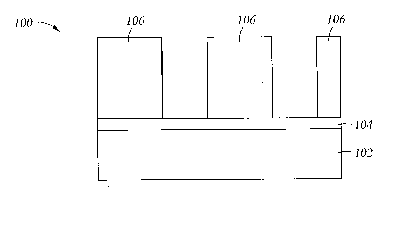
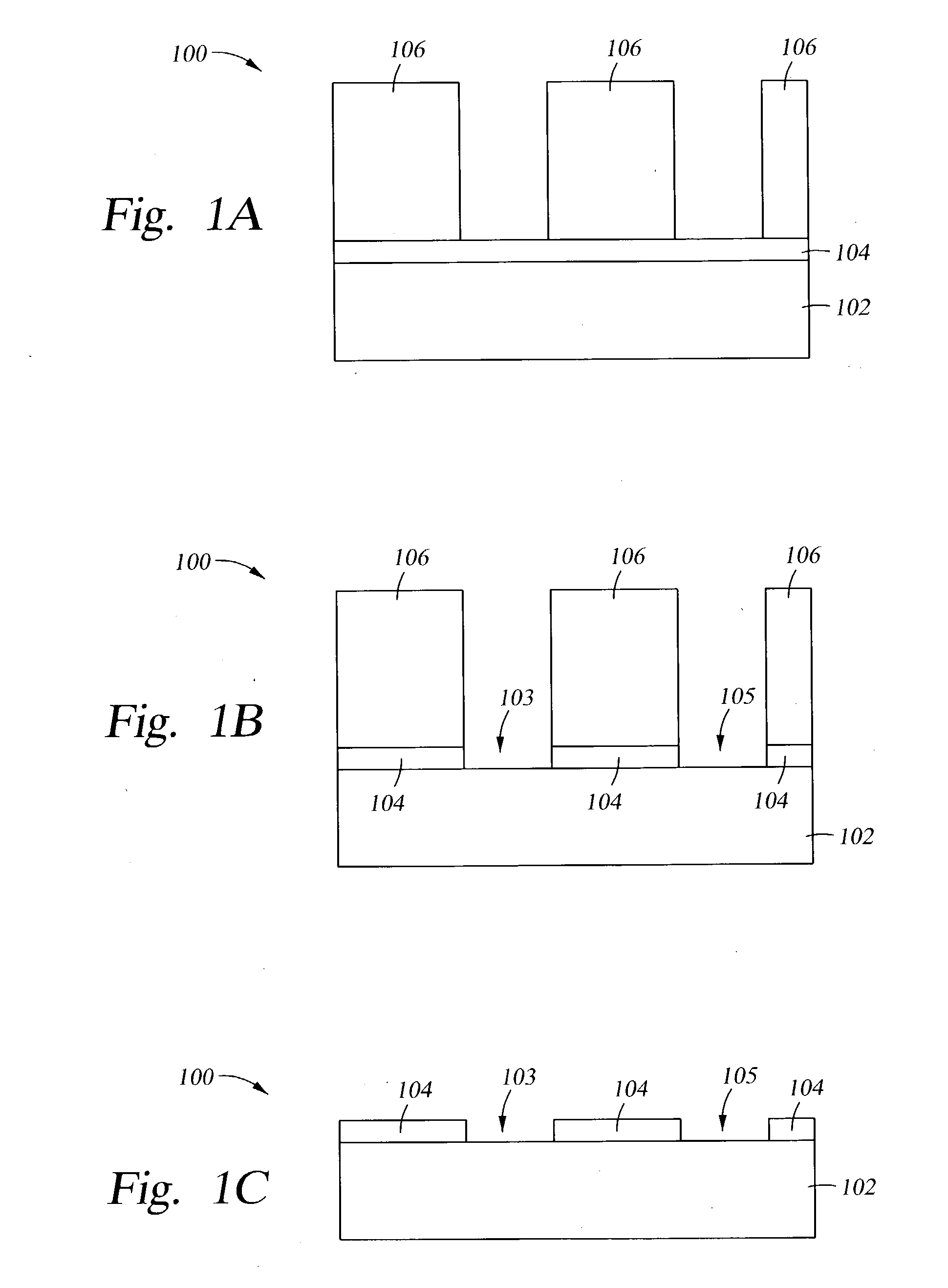
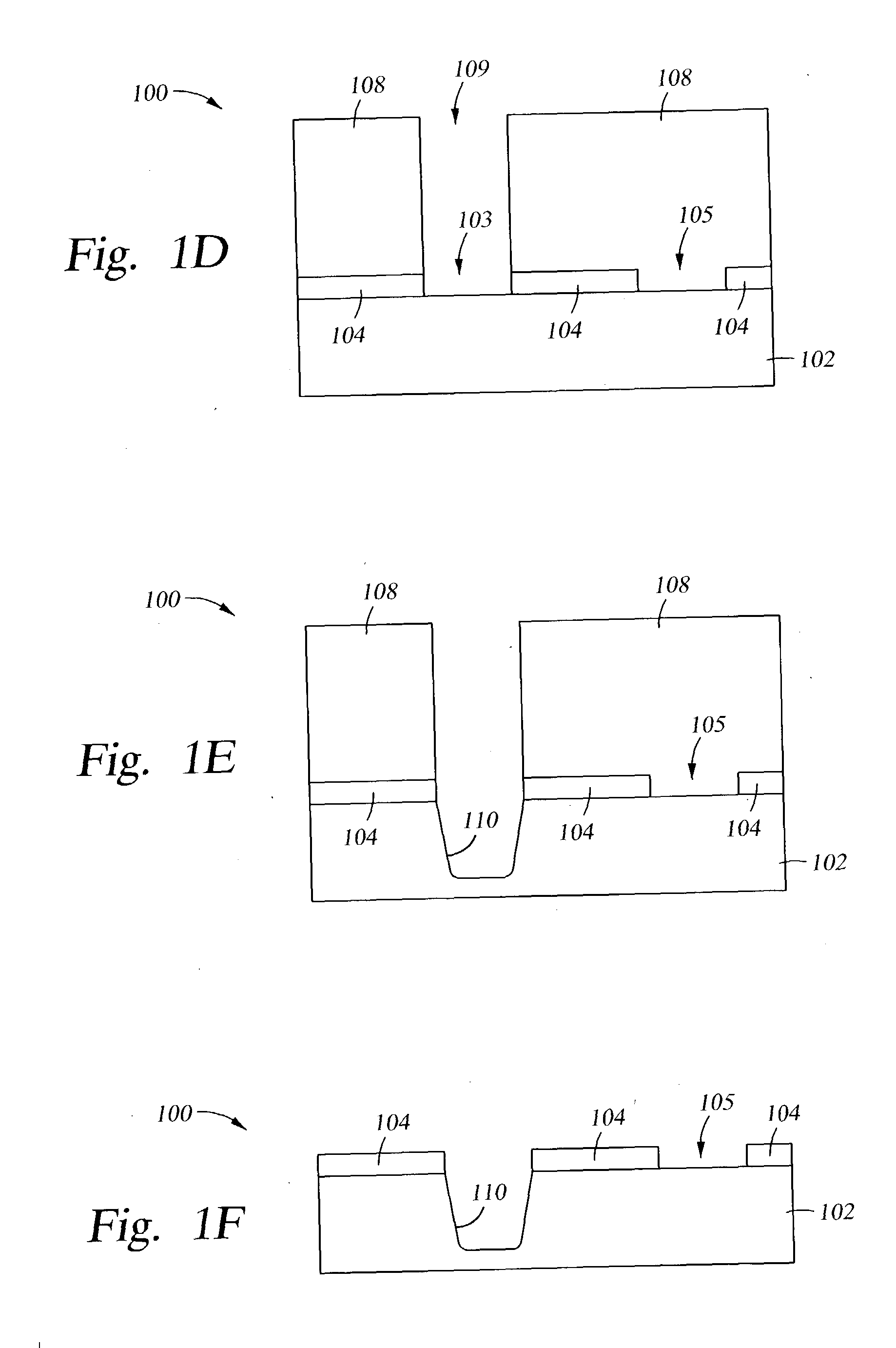
[0026] Disclosed herein is a method of etching features to different depths in a silicon substrate. Exemplary processing conditions for performing various embodiments of the method of the invention are set forth below.

[0027] As a preface to the detailed description, it should be noted that, as used in this specification and the appended claims, the singular forms "a", "an", and "the" include plural referents, unless the context clearly dictates otherwise.

[0028] I. An Apparatus for Practicing the Invention

[0029] The embodiment example etch processes described herein were carried out in a CENTURA.RTM. Integrated Processing System available from Applied Materials, Inc., of Santa Clara, Calif. This apparatus is described in detail below to permit a better understanding of the invention; however, it is contemplated that other apparatus known in the industry may be used to carry out the etching process.

[0030] FIG. 3A shows an elevation schematic of the CENTURA.RTM. Integrated Processing S...


PUM

PropertyMeasurementUnit
roughnessaaaaaaaaaa
roughnessaaaaaaaaaa
roughnessaaaaaaaaaa

Abstract

Disclosed herein is an easy and well-integrated method of etching features to different depths in a crystalline substrate, such as a single-crystal silicon substrate. The method utilizes a specialized masking process and takes advantage of a highly selective etch process. The method provides a system of interconnected, variable depth reservoirs and channels. The plasma used to etch the channels may be designed to provide a sidewall roughness of about 200 nm or less. The resulting structure can be used in various MEMS applications, including biomedical MEMS and MEMS for semiconductor applications.

Description

[0001] 1. Field of the Invention[0002] The present invention pertains to a method of etching features to different depths, and with different etched surface finishes, in a crystalline substrate. In particular, the invention pertains to a method of etching a system of interconnected, variable depth microfluid reservoirs and channels in a crystalline substrate, such as a silicon substrate.[0003] 2. Brief Description of the Background Art[0004] The trend in chemical and biochemical sample analysis, and especially in separation systems such as liquid chromatography and capillary electrophoresis systems, is toward smaller and smaller device dimensions. The smaller dimensions are required in some instances to meet performance requirements, and in other instances provide improved performance or reduced analysis costs. In this regard, miniaturized separation systems provide a variety of benefits as compared with conventional separation systems. Some of these benefits includes: 1) more effec...

Claims


Application Information

Patent Timeline
Patent Type & Authority Applications(United States)
IPC IPC(8): B81C1/00H01L21/3065H01L21/308
CPCB81B2201/0214B81B2201/058B81C1/00626H01L21/3081B81C2201/0132H01L21/3065B81C99/009
Inventor CHINN, JEFFREY D.RATTNER, MICHAEL B.COOPER, JAMES A.GUENTHER, ROLF A.
Owner APPLIED MATERIALS INC
Why Eureka
Try Eureka