Method for reducing roughness of photoresist during electron beam lithography

A technology of electron beam lithography and roughness, which is applied in microlithography exposure equipment, originals for photomechanical processing, optics, etc., can solve the problems of unable to make lines, not high enough, loss, etc., to reduce roughness , Improve stability and reduce the effect of fluctuation changes

Active Publication Date: 2014-03-26
SOI MICRO CO LTD
View PDF4 Cites 4 Cited by
  • Summary
  • Abstract
  • Description
  • Claims
  • Application Information

AI Technical Summary

Problems solved by technology

The thinner the photoresist, the smaller the lines can be exposed. However, such a thin photoresist is often lost early in the etching process due to the insufficient selectivity of the etching process, so that the required photoresist cannot be obtained. lines and have severe line roughness issues

Method used


Image

  • Method for reducing roughness of photoresist during electron beam lithography
  • Method for reducing roughness of photoresist during electron beam lithography
  • Method for reducing roughness of photoresist during electron beam lithography

Examples


Embodiment Construction

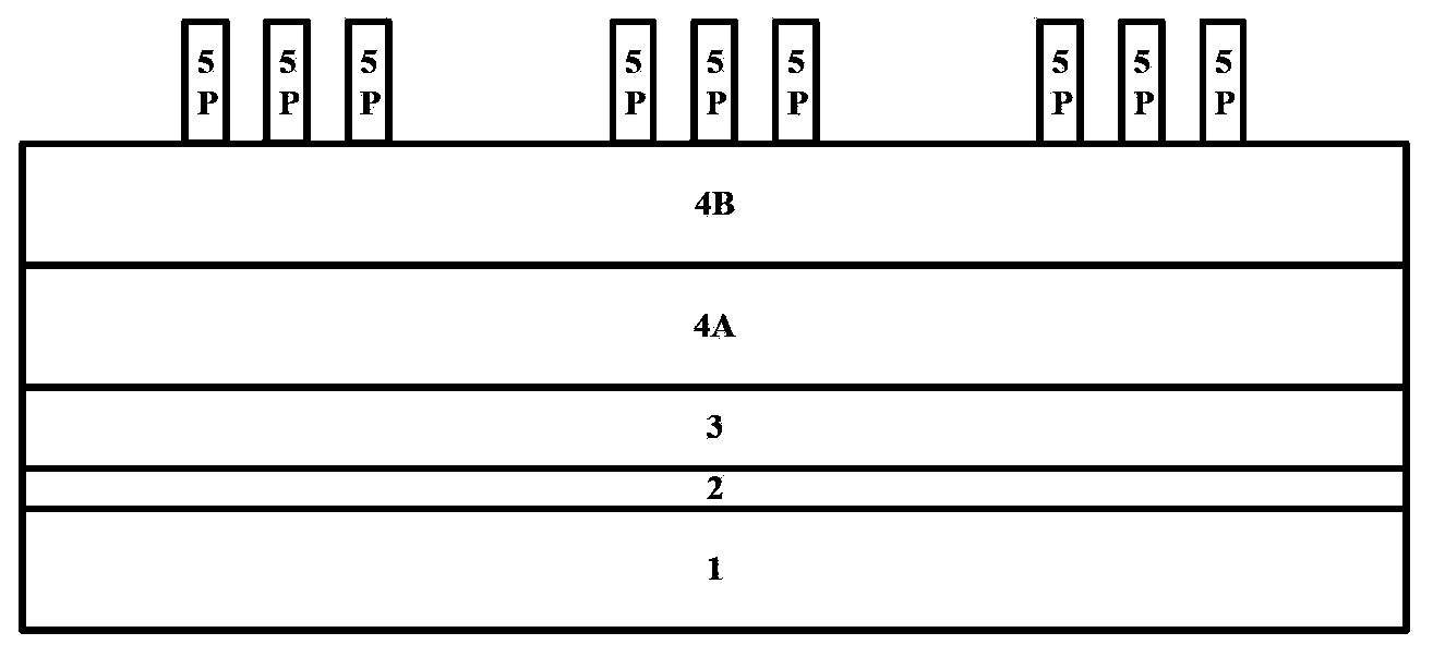
[0021] The features and technical effects of the technical solution of the present invention will be described in detail below with reference to the accompanying drawings and in combination with exemplary embodiments. It should be pointed out that similar reference numerals represent similar structures, and the terms "first", "second", "upper", "lower", "thick", "thin" and the like used in this application can be used for Modify various device structures. These modifications do not imply a spatial, sequential or hierarchical relationship of the modified device structures unless specifically stated.

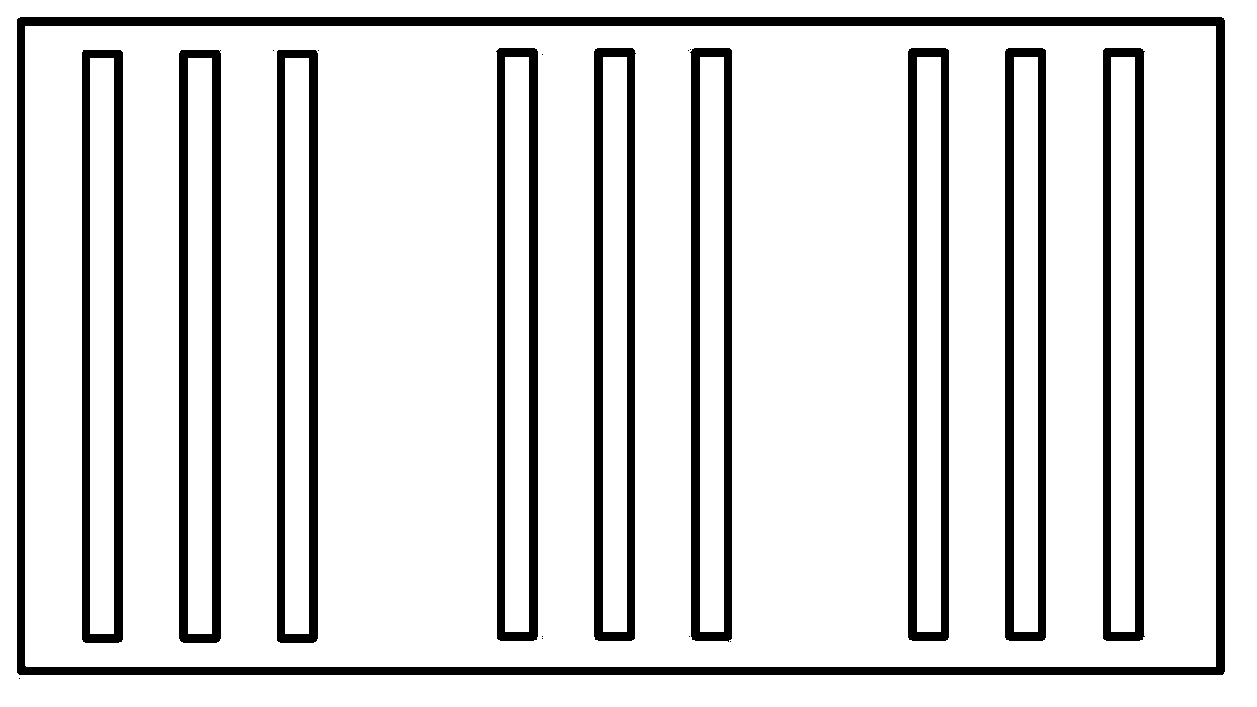
[0022] Reference attached figure 1 , is a schematic top view of a small-linewidth pattern prepared by electron beam technology. Wherein, a plurality of parallel rectangular lines in the illustration represent patterns that need to be exposed by electron beams, and lines with pattern sizes smaller than nodes below 22nm can be prepared. The lines are, for example, lines of variou...


PUM


Abstract

The invention discloses a method for reducing roughness of photoresist during electron beam lithography. The method comprises the steps of forming a structural material layer and a first hard mask layer on a substrate; forming a second hard mask layer on the first hard mask layer; forming an electron beam photoresist pattern on the second hard mask layer; etching the second hard mask layer to form a second hard mask pattern with the electron beam photoresist pattern as a mask; etching the first hard mask layer to form a first hard mask pattern with the second hard mask pattern as a mask; and etching the structural material layer to form a required line with the first hard mask pattern and the second hard mask pattern as masks. According to the method, multiple hard mask layers with different materials and multiple etching operations are adopted, and the roughness of the side wall of the electron-beam photoresist is prevented from being transmitted to the lower structural material layer, so that the line roughness is effectively reduced, the process stability is improved and the fluctuations of device performance are reduced.

Description

technical field [0001] The invention relates to the field of semiconductor integrated circuit manufacturing, in particular to a method for reducing the roughness of resist during electron beam lithography. Background technique [0002] With the gradual reduction of VLSI feature size, the technical limit of ordinary optical exposure has come after entering the 22nm technology generation in the manufacturing method of semiconductor devices. At present, after the 45nm process node, i193nm immersion lithography technology combined with double exposure and double etching technology is generally used to prepare smaller lines. Fine patterning at nodes below 22nm typically requires exposure and lithography using e-beam or EUV. [0003] Regarding EUV lithography technology, it is still in the research and development stage, and there are still several key technologies that need to be overcome and improved, and it cannot be applied to large-scale integrated circuit manufacturing. In...

Claims


Application Information

Patent Timeline
Patent Type & Authority Applications(China)
IPC IPC(8): G03F7/20G03F1/20H01L21/027
Inventor 孟令款贺晓彬李春龙
Owner SOI MICRO CO LTD
Why Eureka
Try Eureka