Cutting method and apparatus for ingot, wafer, and manufacturing method of solar cell

a manufacturing method and technology of solar cells, applied in the direction of sustainable manufacturing/processing, final product manufacturing, etc., can solve the problems of limited thickness, solar cell needs light absorption, and the present status is near a technical limit, so as to achieve the effect of shortening the time for cutting a single crystal ingot, reducing the cost of production, and increasing the thickness

Inactive Publication Date: 2004-03-25
Y Y L
View PDF3 Cites 30 Cited by
  • Summary
  • Abstract
  • Description
  • Claims
  • Application Information

AI Technical Summary

Benefits of technology

0017] When any manufacturing method is established, solar cells using the single crystal silicon will become popular widely. Especially, the solar cells using the single crystal silicon have a conversion efficiency at least twice in comparison with the case of amorphous silicon and can yield the same power at a half area on the roof, showing that it is a very important technical development to develop the solar cell using the single crystal silicon.
0018] Accordingly, it is

Problems solved by technology

However, the present status would be nearly at a technical limit.
The solar cell needs absorption of lig

Method used


Image

  • Cutting method and apparatus for ingot, wafer, and manufacturing method of solar cell
  • Cutting method and apparatus for ingot, wafer, and manufacturing method of solar cell
  • Cutting method and apparatus for ingot, wafer, and manufacturing method of solar cell

Examples


Embodiment Construction

]

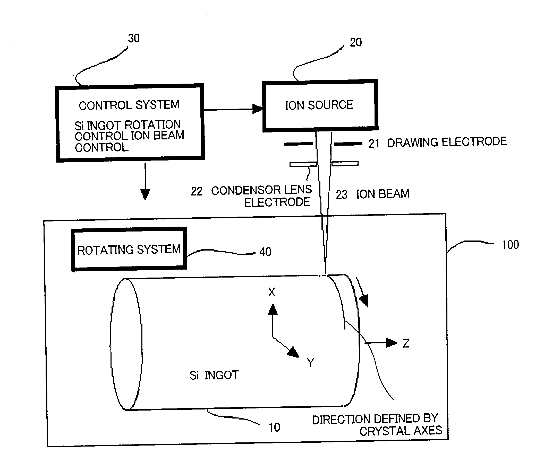
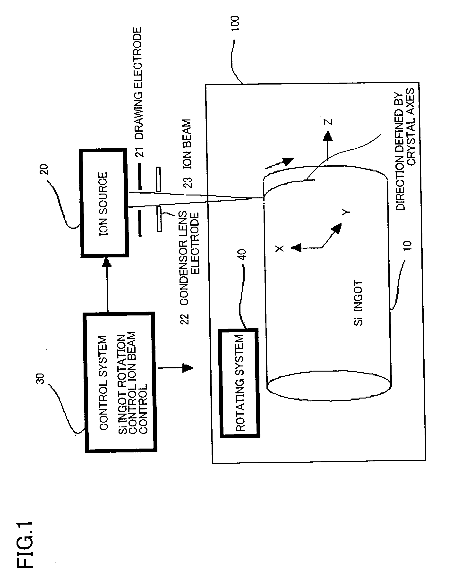
[0072] A preferred embodiment of the present invention is described with reference to the figures. FIG. 1 schematically shows a structure of an embodiment of the present invention. An apparatus according to an embodiment of the present invention comprises an ion source 20, an ion emitting electrode 21 and a condenser lens electrode 22 so as to condense ion beam 23 onto the surface of silicon ingot 10.

[0073] The lattice defects are generated on the surface because the mean free path of ion beam 23 in the surface of silicon ingot is short. The scanning direction of the ion beam 23 is along a "direction defined by crystal axes" (i,e, along a direction of a plane defined by x-and y-axes or a direction defined by a plane transverse to z-axis) of the silicon ingot 10 shown in FIG. 1.

[0074] It is possible that a mask (not shown in the figures) of a pattern having an open part irradiated with ion beam 23 covers silicon ingot 10.

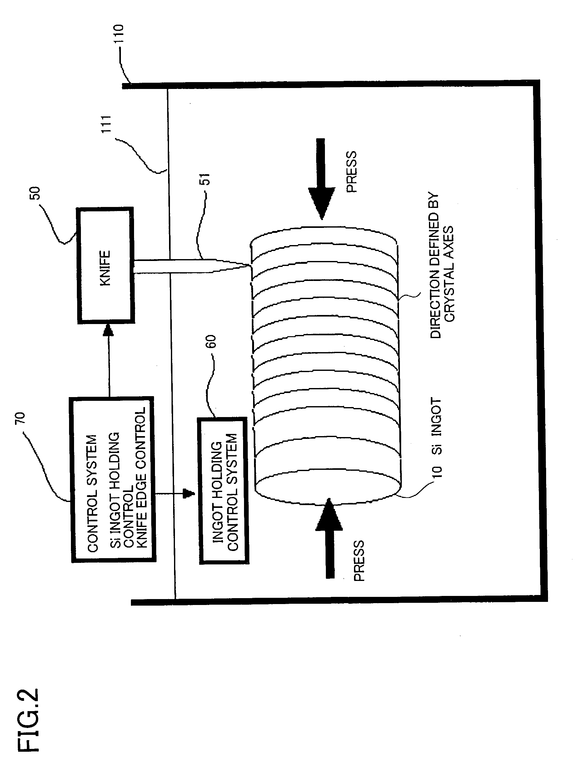
[0075] In producing the approximately cylindrical silicon ingo...


PUM

PropertyMeasurementUnit
Lattice constantaaaaaaaaaa
Crystal structureaaaaaaaaaa
Defectsaaaaaaaaaa

Abstract

Cutting method of ingot into wafers along cleavage plane. Onto surface of single crystal ingot 10 is implanted ion beam 23 to generate lattice defects in a direction defined by the crystal axes that corresponds to the cleavage plane. Cleavage is generated by applying a shock by a knife edge to the position of the lattice having a cutting face as a cleavage plane. Production time of waters is reduced with a more numbers of sliced wafers from one ingot.

Description

[0001] The present invention relates to a method and apparatus for cutting a single crystal ingot, particularly a method and apparatus suitable for manufacturing a solar cell, and a wafer.[0002] Single crystal or polycrystal such as, for example, single crystal Si, amorphous Si or polycrystalline Si is widely used for a optoelectric conversion material (optovoltaic material) to produce solar cells. Because, for example, amorphous Si has a forbidden band as wide as 1.7 eV and an absorption coefficient for visible light as large as ten times of single crystal Si. Additionally the single crystal Si is expensive. A solar cell made from ternary compounds of the chalcopyrite type attracts attention as a high efficiency solar cell material besides silicon, and CdS / CuInSe2 heterojunction polycrystal thin film or the like is eagerly studied, too.[0003] Amorphous Si or polycrystalline Si is made from an single crystal ingot as a base material. Semiconductor devices, memories or logic LSIs suc...

Claims


Application Information

Patent Timeline
IPC IPC(8): B28D5/04B26D7/08B28D5/00H01L21/304H01L31/00H01L31/04H01L31/18
CPCB28D5/00B28D5/0011Y02E10/547Y02B10/12H01L31/1804Y02B10/10Y10T83/0405Y02P70/50
Inventor YAMAGUCHI, SATARO
Owner Y Y L
Why Eureka
Try Eureka