Electroabsorption modulator having a barrier inside a quantum well
- Summary
- Abstract
- Description
- Claims
- Application Information
AI Technical Summary
Benefits of technology
Problems solved by technology
Method used
Image

Examples
Embodiment Construction
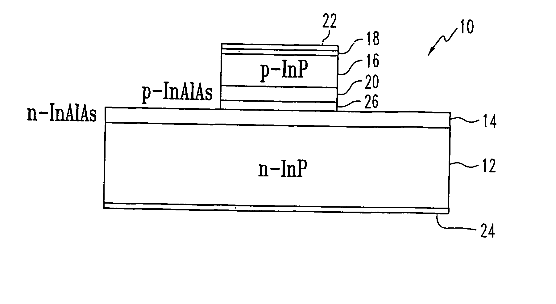
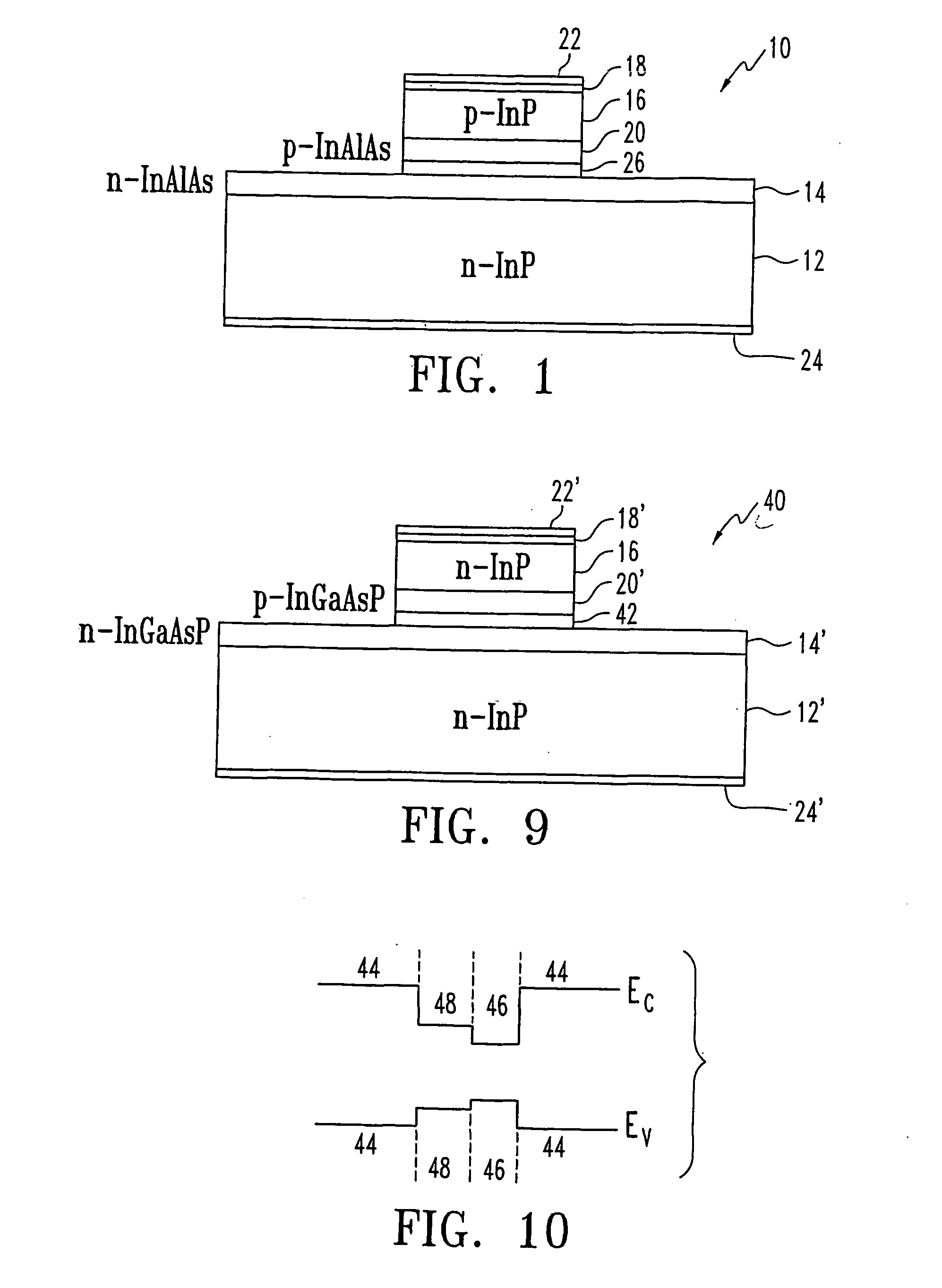
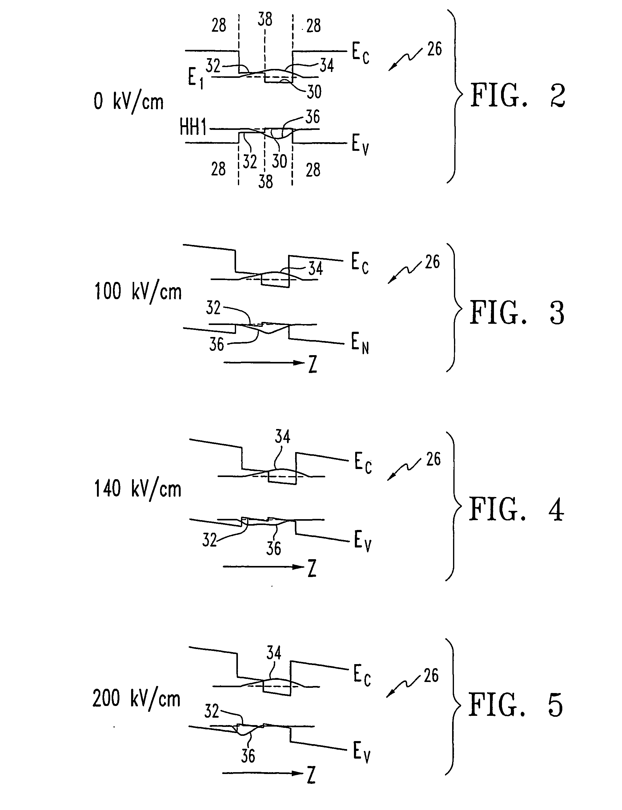
[0020] Turning now to FIG. 1, an electroabsorption modulator (EAM) in accordance with an embodiment of the invention is indicated generally at 10, and includes a n-InP substrate 12 in contact with an n-InAlAs waveguide cladding layer 14 (where n indicates an electron concentration, for example, of approximately 1.times.10.sup.18 cm.sup.-3, in this embodiment). The EAM 10 also includes an p-InP buffer layer 16 provided between a heavily doped p-InGaAs contact layer 18 (where p indicates hole concentration, for example, of approximately 1.times.10.sup.18 cm.sup.-3 in this embodiment) and a p-InAlAs waveguide cladding layer 20 (where p=1.times.10.sup.18 cm.sup.-3). On the surface opposite the p-InP buffer layer 16, the p-InGaAs contact layer 18 is in contact with a positive electrode 22 made of electrically conductive metal alloy such as AuZn followed by gold, for example. Similarly, the surface of the n-InP substrate 12 opposite the waveguide cladding layer 14 is in contact with an n ...
PUM
 Abstract
Description
Claims
Application Information
 - R&D Engineer
- R&D Manager
- IP Professional
- Industry Leading Data Capabilities
- Powerful AI technology
- Patent DNA Extraction
Browse by: Latest US Patents, China's latest patents, Technical Efficacy Thesaurus, Application Domain, Technology Topic.
© 2024 PatSnap. All rights reserved.Legal|Privacy policy|Modern Slavery Act Transparency Statement|Sitemap