Semiconductor device and method

a technology of semiconductor devices and semiconductors, applied in the field of semiconductor devices, can solve the problems of compromising the performance of the semiconductor device, affecting the efficiency of the device, and being somewhat negligible, so as to reduce the surface current, and eliminate the effect of surface leakage curren

Active Publication Date: 2010-09-16
UNIVERSITY OF ROCHESTER
View PDF1 Cites 52 Cited by
  • Summary
  • Abstract
  • Description
  • Claims
  • Application Information

AI Technical Summary

Benefits of technology

[0023]An embodiment of the present invention addresses the needs described above by providing semiconductor devices and assemblies that substantially eliminate surface leakage currents. An embodiment of the present invention addresses the needs described above by providing a method for in situ manufacturing of the aforementioned semiconductor devices that are designed to reduce surface currents, while still producing efficient behaviors of bulk (photo- and dark-) currents. An embodiment of the present invention addresses the needs described above by providing a method that eliminates the need for ex situ surface passivation treatments and their disadvant

Problems solved by technology

Thus, the application of even a large amount of energy will typically not generate a current flow.
One of the issues that detract from the performance of a semiconductor device relates to currents that are not intentionally generated by the device.
Clearly, if the device generates extraneous currents, in addition to those generated by photodetection, the sensitivity of the device will be compromised.
The latter effect is normally somewhat negligible, however, in small bandgap materials, like those used in long wavelength detectors, and the effects may be significant.
The performance of many types of photodetectors fabricated with multiple types of materials is limited by surface l

Method used


Image

  • Semiconductor device and method
  • Semiconductor device and method
  • Semiconductor device and method

Examples


example 1

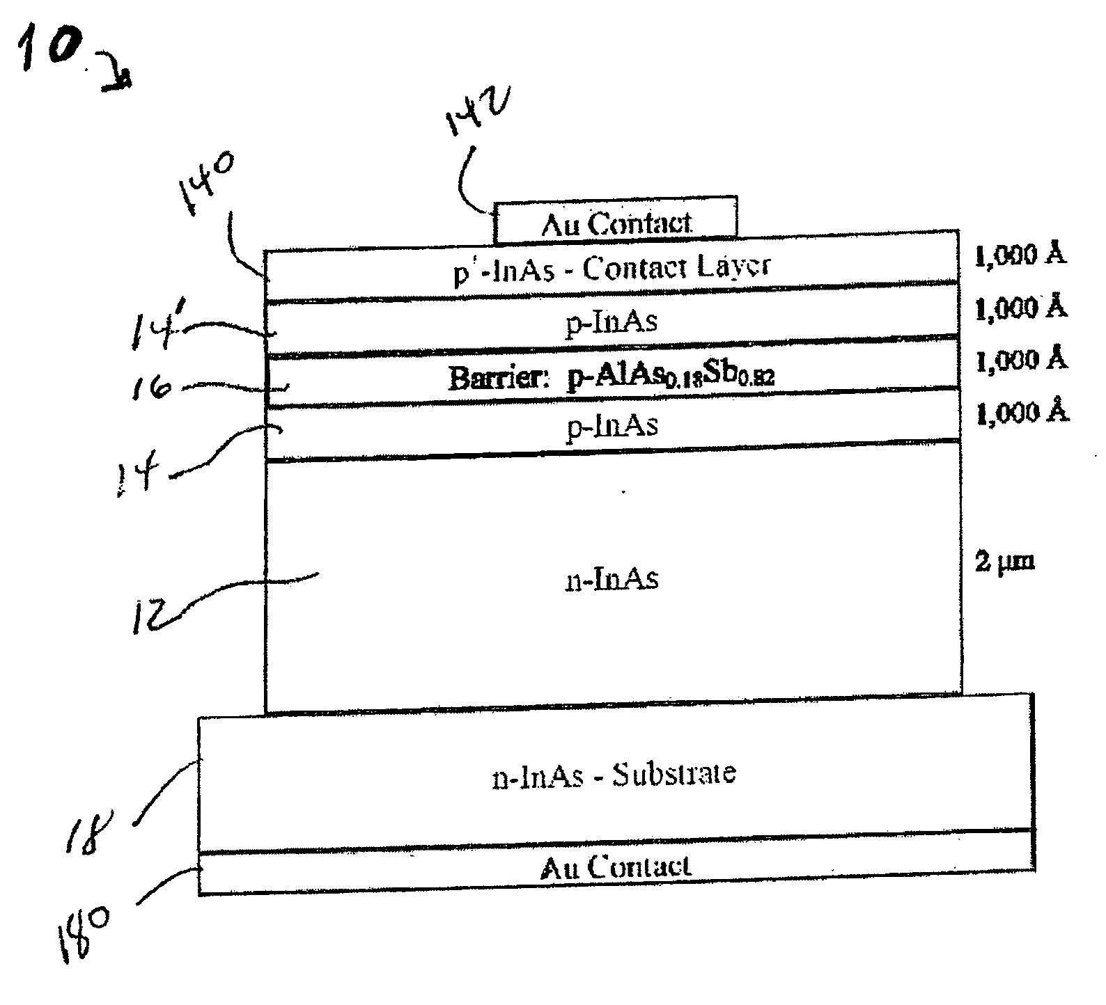
[0054]As embodied herein and depicted in FIG. 9, a cross-sectional diagrammatic view of an InAs photodiode 10 with a unipolar barrier 16 in accordance with one embodiment of the invention is disclosed. In this embodiment, AlAs0.18Sb0.82 has been identified as a suitable unipolar barrier material for InAs semiconductor devices. The photodiodes 10 of the present invention were grown by solid source molecular beam epitaxy (MBE) by a Riber 32P system utilizing As2 and Sb4. First, the devices were grown on unintentionally doped, n-type InAs substrates 18, which were disposed on a gold contact material 180. Next, a 2 μm, unintentionally doped n-type InAs layer 12 having a carrier concentration of n≈1016 cm−3 was deposited on substrate 18. This step was followed by depositing a p-type layer 14. P-type layer 14 is formed by a 1,000 Å (angstrom) layer of beryllium doped p-type InAs with a carrier concentration of p≈1018 cm−3. At this point in the process, a growth stop of about 2 minutes fol...


PUM


Abstract

The present invention is directed to a semiconductor device that includes at least one p-n junction including a p-type material, an n-type material, and a depletion region. The at least one p-n junction is configured to generate bulk photocurrent in response to incident light. The at least one p-n junction is characterized by a conduction band energy level, a valence band energy level and a surface Fermi energy level. The surface Fermi energy level is pinned either near or above the conduction band energy level or near or below the valence band energy level. A unipolar barrier structure is disposed in a predetermined region within the at least one p-n junction. The unipolar barrier is configured to raise the conduction band energy level if the surface Fermi energy level is pinned near or above the conduction band energy level or lower the valence band energy level if the surface Fermi energy level is pinned near or below the valence band energy level such that the unipolar barrier is configured to propagate the bulk photocurrent and substantially block surface leakage current. The at least one p-n junction and the unipolar barrier are integrally formed.

Description

CROSS-REFERENCE TO RELATED APPLICATIONS[0001]This application claims the benefit of priority under 35 U.S.C. §119(e) to U.S. Provisional Patent Application Ser. No. 61 / 152,289 filed on Feb. 13, 2009, the content of which is relied upon and incorporated herein by reference in its entirety.FEDERALLY SPONSORED RESEARCH[0002]This invention was made with government support under Award number FA9550-08-1-0109 sponsored by the Air Force Office of Sponsored Research. The government has certain rights in the invention.BACKGROUND OF THE INVENTION[0003]1. Field of the Invention[0004]The present invention relates generally to the field of electronic devices, and particularly to semiconductor devices.[0005]2. Technical Background[0006]The following descriptions and examples are not admitted to be prior art by virtue of their inclusion within this section.[0007]A photodiode is a type of diode that is configured to convert light of a particular wavelength into either current or voltage, depending ...

Claims


Application Information

Patent Timeline
IPC IPC(8): H01L31/102H01L21/02
CPCB82Y20/00H01L31/1032H01L31/035281Y02E10/544H01L31/1035Y02E10/50
Inventor WICKS, GARY W.
Owner UNIVERSITY OF ROCHESTER
Why Eureka
Try Eureka