

Antimonide II superlattice infrared detector with planar structure and preparation method thereof
A technology of infrared detectors and planar structures, applied in semiconductor devices, final product manufacturing, sustainable manufacturing/processing, etc., can solve problems such as limited effects, unfinished processes, surface leakage currents of conductive channels on the surface of side walls, etc., to achieve Best performance, no surface leakage current, high reliability
- Summary
- Abstract
- Description
- Claims
- Application Information
AI Technical Summary
Problems solved by technology
Method used
Image

Examples
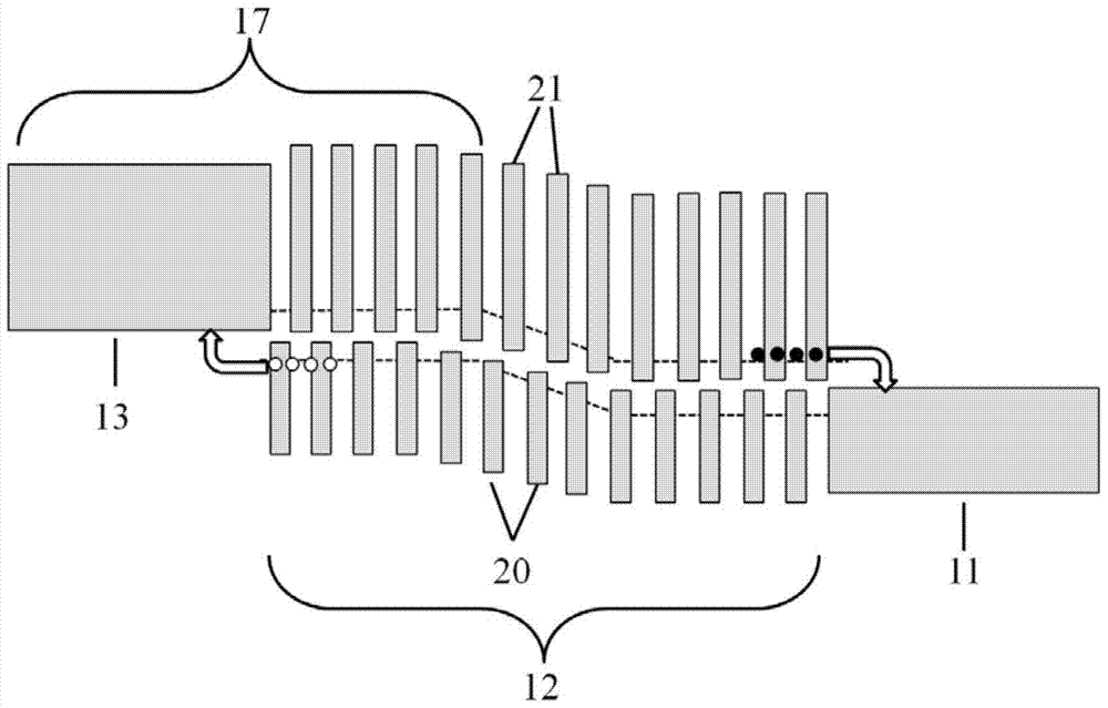
Embodiment 1
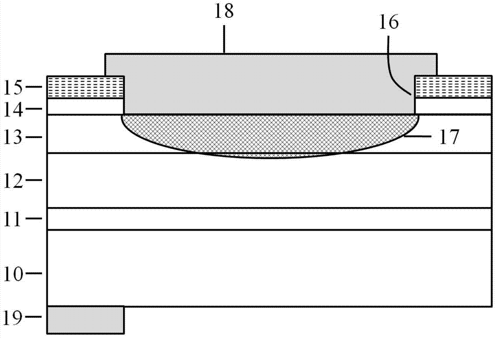
[0055] Embodiment 1 uses metal-organic chemical vapor deposition (MOCVD) as a growth process to provide an n-type InAs substrate 10, and the growth sources are TMGa, TMIn, TMSb and AsH 3 , the dopant source n-type is Si 2 h 6 , p-type is DEZn. The growth temperature is about 530° C., and the reaction chamber pressure is 100 Torr. After high temperature treatment to remove impurities on the surface of the substrate, according to figure 1 The IR detector structure shown is grown sequentially:
[0056] (1) 0.5 μm InAs buffer layer 11, doped with Si, the concentration is 5×10 17 cm -3 ;
[0057] (2) 500-period InAs / GaSb superlattice absorption layer 12, InAs thickness is 4.8nm, GaSb thickness is 3nm, that is, the total thickness is 3.9μm, only Si is doped in InAs, and the average concentration is 2×10 16 cm -3 ;
[0058] (3) 100-period InAs / GaSb superlattice contact layer 13, the thickness of InAs is 3nm, the thickness of GaSb is 3nm, that is, the total thickness is 0.6μm...
Embodiment 2
[0062] Embodiment 2 uses molecular beam epitaxy (MBE) as the growth process to provide an n-type GaSb substrate 10, the growth source is solid single source Ga, In, As and Sb, and the n-type dopant source is Te. The growth temperature is about 450°C. After the substrate is degassed and impurity removed, according to the following figure 1 The IR detector structure shown is grown sequentially:
[0063] (1) 1.5 μm InAsSb buffer layer 11, doped with Te, the concentration is 1×10 17 cm -3 ;
[0064] (2) 600 cycles InAs / InAs 0.6 Sb 0.4 Superlattice absorption layer 12, InAs thickness 7nm, InAs 0.6 Sb 0.4 The thickness is 2nm, that is, the total thickness is 5.4μm, doped with Te, the concentration is 2×10 15 cm -3 ;
[0065] (3) 4μm GaSb contact layer 13, doped with Te, the concentration is 5×10 16 cm -3 ;
[0066] (4) 0.5 μm unintentionally doped AlGaSb passivation layer 14;
[0067] After the growth was completed, 2 μm SiO was deposited on the epitaxial wafer by plas...
PUM
 Abstract
Description
Claims
Application Information