Nanotube transistor device

a transistor and nanotube technology, applied in the field of nanotube transistor devices, can solve the problems of lack of reproducibility of devices, inability to yield consistent device characteristics, and inability to demonstrate devices described so far to achieve consistent device characteristics

Inactive Publication Date: 2005-03-10
KIM BYONG MAN +2
View PDF7 Cites 58 Cited by
  • Summary
  • Abstract
  • Description
  • Claims
  • Application Information

AI Technical Summary

Benefits of technology

[0011] The nanotube structure may comprise first and second and more generally n nanotubes one within the other and the locally doped region may extend into one or some of the nanotubes but not the or each of the others. Alternatively the locally doped region may extend into both or all of the nanotubes.
[0012] The doped region may comprise a semiconductor providing a conduction band barrier that can be controlled by an external voltage applied to the gate region, to control conduction along the path between the source and drain.
[0013] The doped region may also comprise a conductor that forms a Schotkky junction in the nanotube structure that can be controlled by an external voltage applied to the gate region to control conduction along the path between the source and drain.

Problems solved by technology

The structures described so far are demonstration devices and not apt to yield consistent device characteristics.
Chemical doping of carbon-nanotube structures has been proposed by C. Zhou, Science, 290, 1552 (2000) to B. Yakobson. Also, a method of forming a heterojunction in a nanotube structure by means of a heat induced solid-solid diffusion and chemical reaction is described in U.S. Pat. No. 6,203,864 to Y. Zhang and S. Iijima. However, these junction forming techniques are not particularly suited to forming transistor structures.
The transistor action results from heterojunctions formed by structural defects in the vicinity of the confluence of the arms of the Y-shaped nanotube and so the device lacks reproducibility.
However, vertical nanotube structures are known to include a high density of various defects and exhibit poor semiconductor properties, degrading performance of the transistor.

Method used


Image

  • Nanotube transistor device
  • Nanotube transistor device
  • Nanotube transistor device

Examples


Embodiment Construction

[0051] Overview

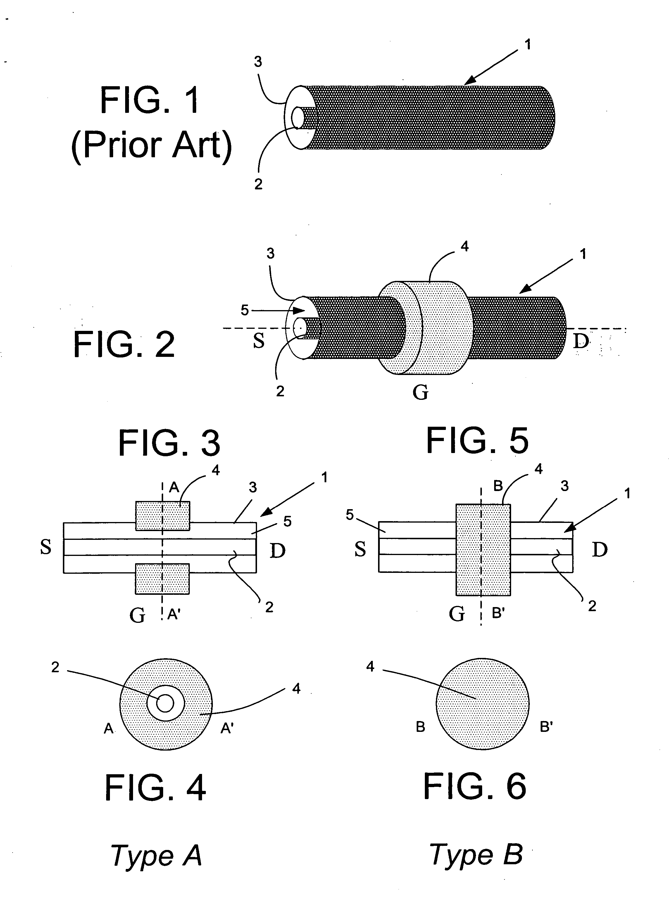
[0052]FIG. 1 illustrates a conventional nanotube structure formed according to any one of the previously described known methods. In this example, nanotube structure 1 comprises first and second generally concentric nanotubes 2, 3 fabricated e.g. from a graphene sheet. The diameters of the tubes 2, 3 are on a nanometer scale, as previously described. In this example, two nanotubes are shown although in practice, the nanotube structure 1 may include only one or many such nanotubes, one within the other.

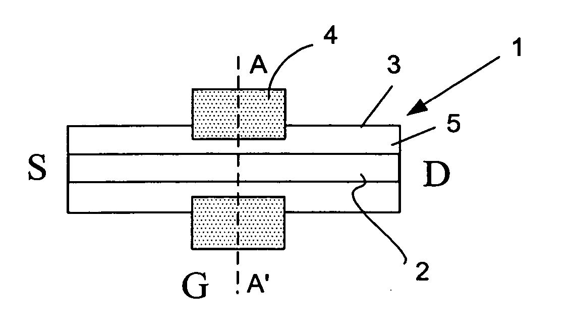
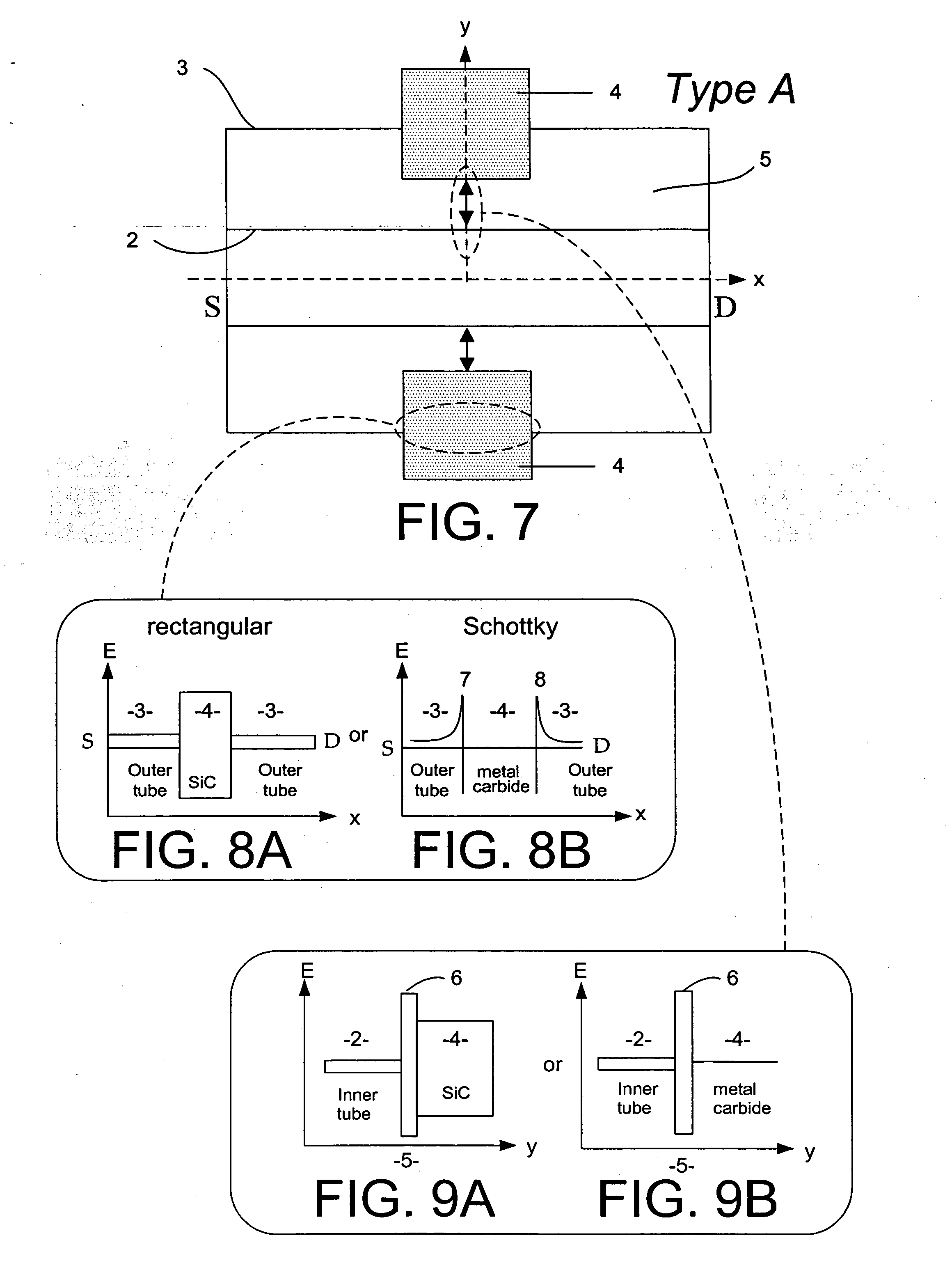
[0053]FIG. 2 illustrates how such a nanotube structure can be modified so as to form the basis of a transistor in accordance with the invention. The energy bandgap and / or the band profile of the nanotube structure 1 is modified locally in region 4 so as to modify the electrical properties of the nanotube structure 1. The resulting structure provides a channel between source and drain regions S, D and the characteristics of the modified region are controlled by a gate G...


PUM


Abstract

A transistor device comprising source and drain regions (S, D), a nanotube structure (2, 3) providing a path for electrical charge carriers between the source and drain regions, and a gate region (4). The nanotube structure has its conduction band structure locally modified in the gate region, e.g. by doping, for controlling the passage of the charge carriers in the path. The device can be used as a flash memory or as a memory element in a DRAM.

Description

FIELD OF THE INVENTION [0001] This invention relates to a transistor device employing a nanotube. BACKGROUND OF THE INVENTION [0002] Nanotubes comprise nanometer scale tubular structures, typically made from a sheet of carbon atoms known as a graphene. They may be single wall or multi-wall structures. A single-walled carbon nanotube typically comprises an elongated, single hollow tube that is about 1 nm in diameter and few-hundreds-nm to few-hundreds-μm in length. A multi-walled carbon nanotube consists of a plurality of generally concentric, hollow tubes of different diameters that can range up to a few hundreds of nanometers. One popular method of synthesizing high quality carbon-nanotube structures uses a chemical vapour deposition technique based on a vapour-solid interaction of methane and hydrogen with a catalyst in a heated environment, as described by J. Kong, H. T. Soh, A. Cassell, C. F. Quate, H. Dai, Nature, 395, 878 (1998). A carbon-nanotube structure can act as a semico...

Claims


Application Information

Patent Timeline
Patent Type & Authority Applications(United States)
IPC IPC(8): G11C13/02B82B1/00H01L21/337H01L21/338H01L21/8247H01L27/115H01L29/06H01L29/74H01L29/786H01L29/788H01L29/792H01L29/808H01L29/812H01L51/30H01L51/40
CPCB82Y10/00G11C13/025G11C2213/18H01L51/0545H01L51/0048H01L51/0508H01L51/002H10K71/30H10K85/221H10K10/46H10K10/466
Inventor KIM, BYONG MANNAKAZATO, KAZUOMIZUTA, HIROSHI
Owner KIM BYONG MAN
Why Eureka
Try Eureka