Conductive component manufacturing process employing an ink jet printer

a technology of ink jet printer and conductive component, which is applied in the direction of conductive pattern formation, circuit masks, printing, etc., can solve the problems of high cost and complexity of the foregoing circuit board manufacturing process, damage to components, and alter the desirable characteristics of the substrate, so as to reduce the cost and enhance the connection density

Inactive Publication Date: 2004-04-22
HEWLETT PACKARD DEV CO LP
View PDF5 Cites 17 Cited by
  • Summary
  • Abstract
  • Description
  • Claims
  • Application Information

AI Technical Summary

Benefits of technology

0008] Among the numerous problems in the art which are addressed by the processes of the present invention is a reduction in the expense associated with currently employed prototyping processes. Further, resistors and capacitors are more fully integrated as opposed to soldered components which easily beco

Problems solved by technology

The attachment of such components generally occur at high temperatures which can damage the components or alter the desirable characteristics of the substrate to which they are applied.
As can be appreciated, the foregoing circuit board manufacturing process is ex

Method used


Image

  • Conductive component manufacturing process employing an ink jet printer
  • Conductive component manufacturing process employing an ink jet printer
  • Conductive component manufacturing process employing an ink jet printer

Examples


Embodiment Construction

[0018] The following description of the preferred embodiment(s) is merely exemplary in nature and is in no way intended to limit the invention, its application, or uses.

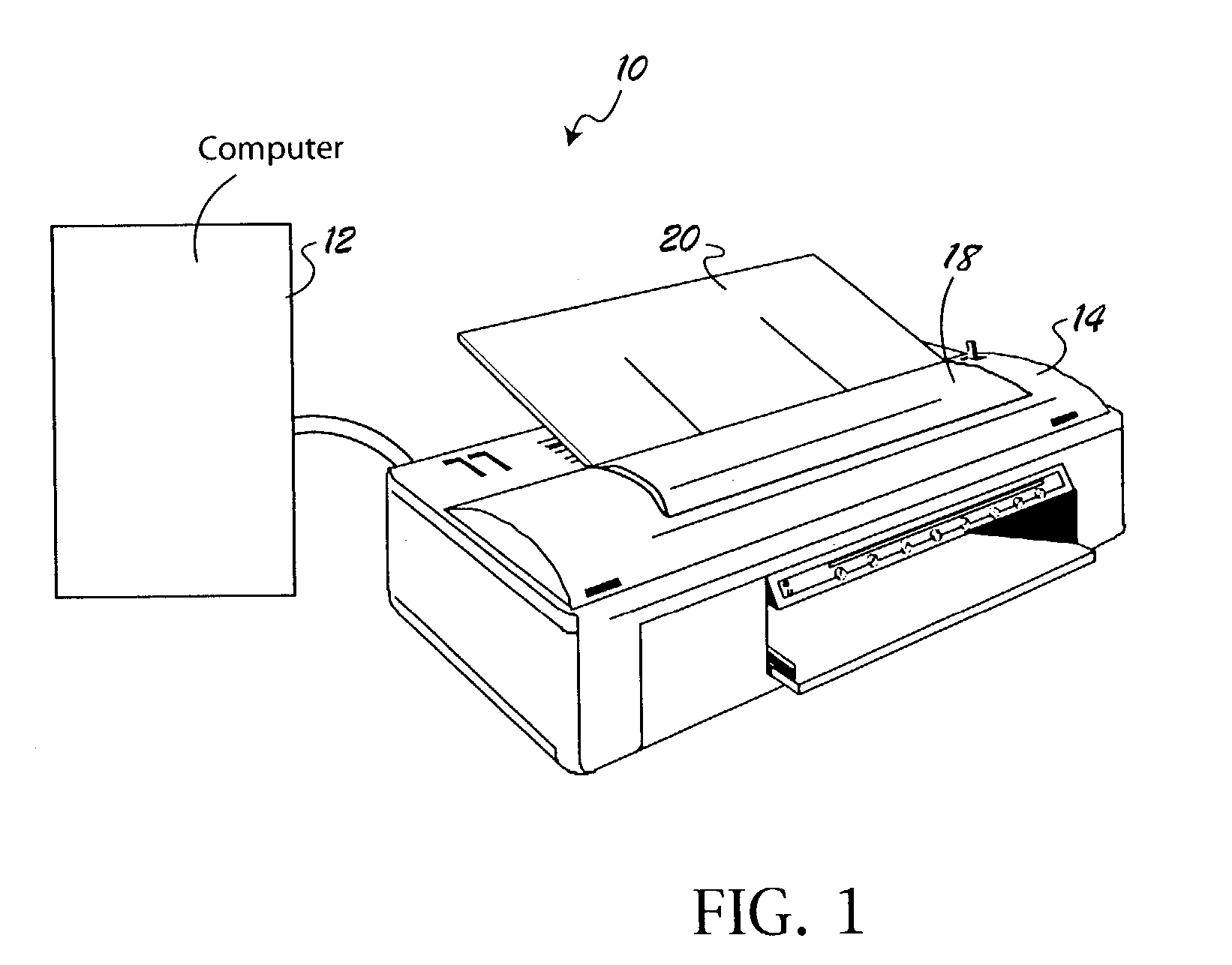
[0019] Referring to FIG. 1, there is shown a manufacturing system assembly 10 including a computer 12 and a conventional desk top direct transfer printer such as an ink jet printer 14. The computer may be selected from many commercially available models or may be custom built provided that the computer includes a microchip or is software compatible to provide the printer with the appropriate signals to carry out the desired printing function.

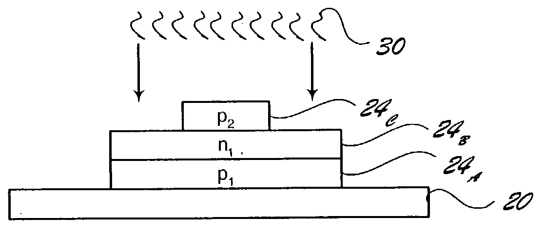
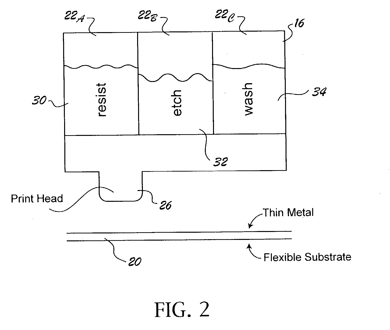
[0020] The printer 14 is generally a commercially available ink jet printer model including as key components a print cartridge 16 as shown in FIG. 2, otherwise referred to herein as a transfer medium cartridge and at least one tray 18 for hosting the printable substrate sheets 20. Although an embodiment employing what is commonly referred to as an ink cartridge is not shown, it ...


PUM


Abstract

The present invention relates to conductive components manufacturing processes employing conventional direct transfer printers to make components such as printer circuit boards and semiconductors, by way of non-limiting example. The process disclosed allow for the production of customized conductive components, particularly prototype components, utilizing in a convenient, cost effective manner.

Description

FIELD OF THE INVENTION[0001] The present invention relates to a conductive component manufacturing processes and, more particularly, to processes for manufacturing conductive components such as circuit boards and semiconductors employing a direct transfer printer such as an ink jet printer.BACKGROUND OF THE INVENTION[0002] Conductive components such as circuit boards are generally processed in sterile environments by complex robotic apparatuses. For example, circuit boards are currently manufactured by applying a vast array of small components such as resistors via soldering to an etched metal board. The attachment of such components generally occur at high temperatures which can damage the components or alter the desirable characteristics of the substrate to which they are applied. As can be appreciated, the foregoing circuit board manufacturing process is expensive and complex in that specialized robotic apparatuses must be designed and used for both prototyping and product manufa...

Claims


Application Information

Patent Timeline
IPC IPC(8): B41J2/01H05K3/00H05K3/06H05K3/12
CPCB41J2/01H05K3/0079H05K2203/013H05K3/067H05K3/125H05K3/061
Inventor ELLIOTT, STEPHEN J.
Owner HEWLETT PACKARD DEV CO LP
Why Eureka
Try Eureka