
Noncontact measuring system for electrical conductivity

a non-contact, measuring system technology, applied in the direction of instruments, semiconductor/solid-state device testing/measurement, flaw detection using microwaves, etc., can solve the problem that the four-point probe method cannot be adopted for on-line inspection, the surface of the wafer is not clear, and the spatial resolution is low

Inactive Publication Date: 2004-05-27
TOHOKU TECHNO ARCH CO LTD
View PDF11 Cites 25 Cited by
  • Summary
  • Abstract
  • Description
  • Claims
  • Application Information

AI Technical Summary

Problems solved by technology

Though the four-point probe method has an advantage of the quite easy measurement, there is a problem that a leading end of the probe hurts a surface of the wafer because it is necessary that the leading end of the probe is in contact with the wafer during the measurement.
Therefore, the four-point probe method can not be adopted for on-line inspection in a manufacturing process of the silicon wafer or non-destructive inspection prior to the manufacturing of the device, and a spot check of few pieces of the silicon wafer products is the only way to inspect the silicon wafer.
The technique using the coil also has the problem of low spatial resolution, so that it is not suited for the non-destructive inspection of the wafer prior to the manufacturing of the device.
However, the quantitative evaluation of the electrical conductivity of the semiconductor wafer has not been successful yet due to influence of the permittivity and thickness of the wafer, or the like.

Method used


Image

  • Noncontact measuring system for electrical conductivity
  • Noncontact measuring system for electrical conductivity
  • Noncontact measuring system for electrical conductivity

Examples


concrete example

[0056] Concretely the measurement was performed by using the n-type of silicon wafer having the diameter of 100 mm and the thickness of 525 .mu.m as the test piece. A radius of the central conductor 148 in the used coaxial cable sensor was 0.15 mm and an inner radius of the external conductor 146 was 0.47 mm.

[0057] The average electrical conductivity of the wafer measured by the four-point probe method was 14.73 S / m. The stand-off distance between the sensor and the test piece was constantly set to 200 .mu.m. The frequency was set to 110 GHz, and the amplitude A of the reflectivity was measured. Paying attention to the temperature dependence of the electrical conductivity, all the measurements were performed under the condition of the room temperature of 25.degree. C.

[0058] FIG. 6 is the measurement result of the electrical conductivity along a diameter direction of the wafer, which is obtained by the four-point probe method. It is found that the central portion has a slightly large...


PUM


Abstract

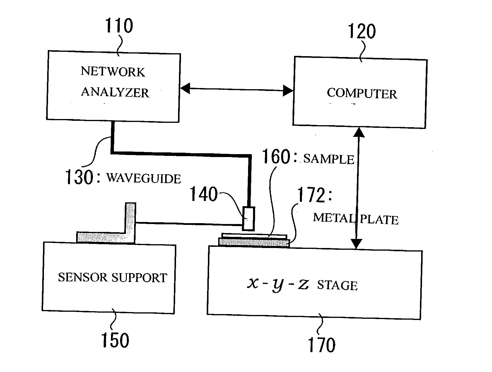
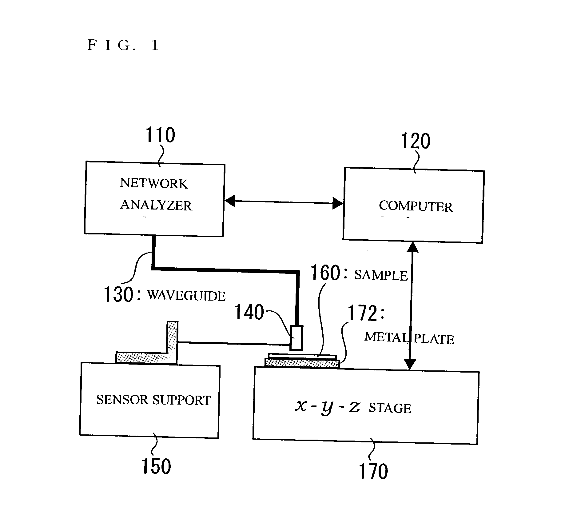
The invention provides a noncontact measuring system for electrical conductivity, which uses a microwave. In the measuring system for electrical conductivity, the microwave generated in a network analyzer (NA) 110 is guided to a surface of a silicon wafer (sample) 160 through a waveguide 130 and a sensor 140. The surface of the silicon wafer 160 is irradiated with the microwave, and the sensor 140 receives the reflected microwave. The electrical conductivity of the silicon wafer 160 is measured in such a manner that a computer (personal computer) 120 calculates the electrical conductivity from an amplitude ratio A and phase difference theta to a reflected wave of the silicon wafer 160, which is determined with the network analyzer 110. The computer 120 performs not only the calculation of the measurement but also whole control of the measuring system such as positioning of the sample.

Description

[0001] 1. Field of the Invention[0002] The present invention relates to an electrical conductivity measuring system for a material, particularly relates to the electrical conductivity measuring system on a noncontact basis, in which a microwave is used.[0003] 2. Description of the Prior Art[0004] Measurement of the electrical conductivity is essential in quality control and performance evaluation of a silicon wafer which is a typical material used for electronic devices.[0005] A four-point probe method is conventionally adopted as the measuring method for the electrical conductivity of the silicon wafer. Though the four-point probe method has an advantage of the quite easy measurement, there is a problem that a leading end of the probe hurts a surface of the wafer because it is necessary that the leading end of the probe is in contact with the wafer during the measurement. Calibration of a thickness of the wafer is also required in quantitative evaluation. Therefore, the four-point ...

Claims


Application Information

Patent Timeline
IPC IPC(8): G01R27/02G01N22/00G01N22/02G01R27/06G01R27/26G01R31/311H01L21/66
CPCG01N22/02G01R31/311G01R27/2658G01R27/06
Inventor JU, YANGSAKA, MASUMIABE, HIROYUKI
Owner TOHOKU TECHNO ARCH CO LTD
Learn More