Applications of nano-enabled large area macroelectronic substrates incorporating nanowires and nanowire composites

a macroelectronic substrate and nanowire technology, applied in nanoinformatics, instruments, burglar alarm mechanical actuation, etc., can solve the problems of incompatibility with low temperature substrates, inability to withstand high temperature, and high cost of processes

Active Publication Date: 2004-06-17
ONED MATERIAL INC
View PDF41 Cites 371 Cited by
  • Summary
  • Abstract
  • Description
  • Claims
  • Application Information

AI Technical Summary

Benefits of technology

0017] The result is a revolutionary new high-performance large-area macroelectronics technology on a variety of substrates, for example plastics, that: (1) outperforms single-crystal silicon wafers (.mu.>5,000 cm.sup.2 / V.multidot.s and on / off current ratio I.sub.on / I.sub.off>10.sup.7 with a threshold potential V.sub.on<1 V); (2) can be applied to extremely large surface areas (A>10 m.sup.2); (3) has the flexibility of polymer electronics (radius of curvature r<1 mm); and / or (4) can be processed and patterned using traditional large-area semiconductor processing techniques like those used to process amorphous silicon, as well as advanced lithographic techniques such as roll-to-roll screen-printing.
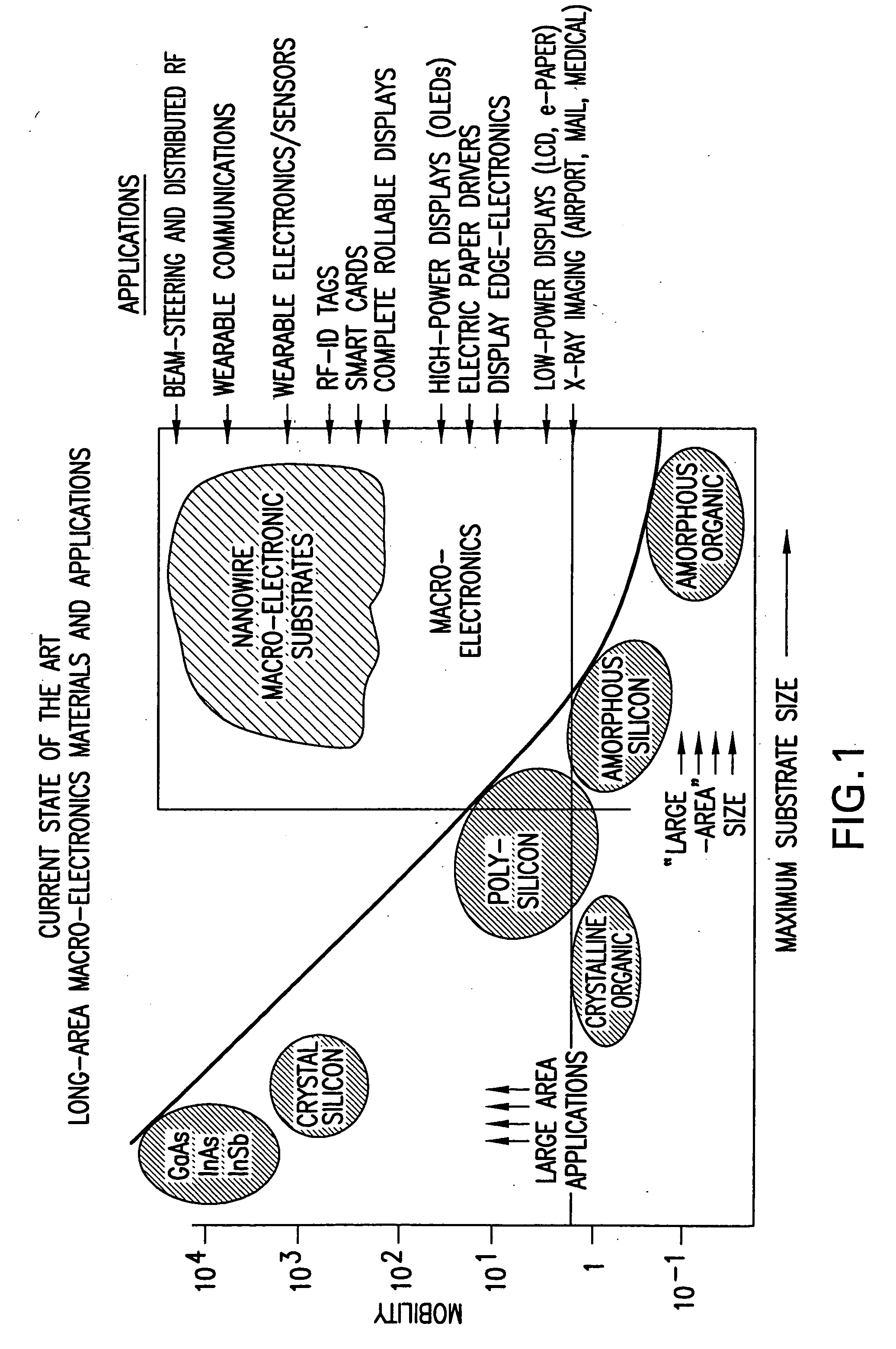
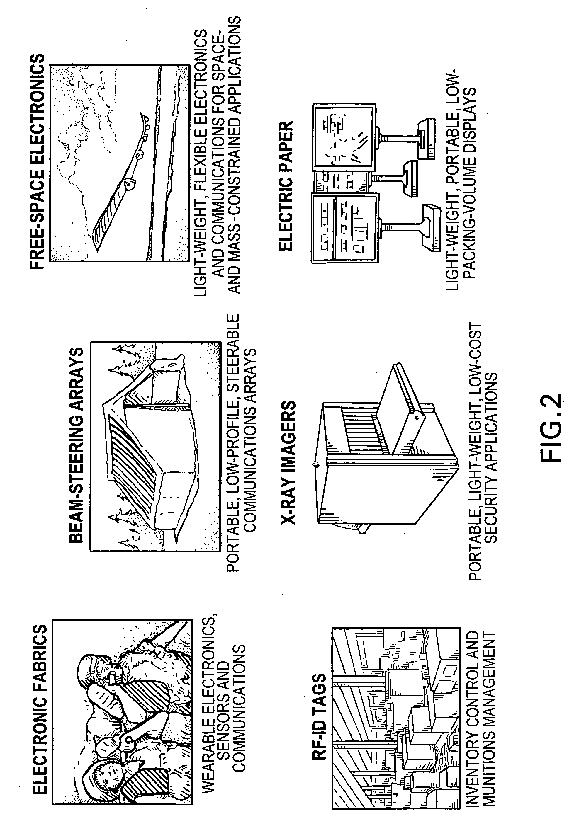
0018] This technology combines the extraordinary conductive properties of a new type of nanomaterial (inorganic semiconductor nanowires) with large-area macroelectronics by producing dense films of preferentially oriented nanowires that span the gap between each source and drain electrode within a device. The result is an electronic material for use in large-area macroelectronics with mobility (.mu.) and current capacity (J) equal to or greater than that of single-crystal silicon. By incorporating alternative nanowire materials such as InAs or GaAs, even higher-performance substrates can be realized. This new-material technology (referred to herein as dense, inorganic and oriented nanowire (DION) thin-film technology and mixed-composition DION thin-film technology) can fill the void in large-area electronic materials (as shown at FIG. 1) to enable the full vision of macroelectronics in commercial, military, and security application. For example, FIG. 2 shows several potential applications of true high-performance macroelectronics.

Problems solved by technology

However, amorphous silicon and organic semiconductors have performance limitations.
Polysilicon has showed improved performance, but requires relatively expensive processes, such as laser induced annealing, and is incompatible with low temperature substrates, such as cheap glass and plastics.
Traditional materials either have high performance but small substrate sizes (e.g., GaAs), or larger sizes with low performance (e.g., amorphous silicon or organics).
Current electronic materials can only access the most primitive large-area macroelectronics applications.
This leaves a tremendous void in materials characteristics, which has prevented the development of the highest-value macroelectronic applications, such as wearable communications and electronics, distributed sensor networks, and radio frequency (RF) beam-steering systems, to name a few.
InAs wafers, however, are currently limited to a maximum of 3-4 inches (8-10 cm) in diameter and are extremely brittle, making them inappropriate for use in such large-area distributed electronic circuits.
As such, the only methods currently available for fabricating such large-area circuits are to wire-bond or solder discrete transistors and components on the large-area active reflector, a costly and failure-prone alternative with inherent performance and efficiency limitations.
Today, even military applications of such arrays are limited to such examples as solid communications arrays on Navy destroyers; they cannot be implemented into mobile, let alone man-portable, communications systems.
A limiting factor in the area of RFID tag tracking systems is the cost of the tags.
Further limiting factors include the distance between the reader and tags, and the orientation of tag antennas relative to the reader antenna.
Current tag and reader technology is not capable of reading such a large number of items in a few seconds.
However, such technology is limited to relatively small size devices, such as headphones, and cannot be applied to the large objects mentioned above.

Method used


Image

  • Applications of nano-enabled large area macroelectronic substrates incorporating nanowires and nanowire composites
  • Applications of nano-enabled large area macroelectronic substrates incorporating nanowires and nanowire composites
  • Applications of nano-enabled large area macroelectronic substrates incorporating nanowires and nanowire composites

Examples


Embodiment Construction

[0099] Introduction

[0100] In many ways, the electronics industry today is in the same position it was fifty years ago. At that time, the introduction of discrete transistors provided the world with unprecedented functionality. By integrating multiple discrete transistors together, functionality was further increased, leading to the broad availability of portable electronics. Unfortunately, at that time, integration was done by hand, causing the electronics industry to rapidly reach a plateau, beyond which integrating more than a few thousand individual transistors became prohibitive in terms of cost and yield. This phenomenon was referred to as the "Tyranny of Numbers".

[0101] This practical limit, resulting from the need for heterogeneous integration of multiple discrete components, brought the integrated electronics industry to a standstill that was only resolved through the invention of a revolutionary new concept: the silicon microcircuit. The silicon microcircuit allowed seamles...


PUM


Abstract

Macroelectronic substrate materials incorporating nanowires are described. These are used to provide underlying electronic elements (e.g., transistors and the like) for a variety of different applications. Methods for making the macroelectronic substrate materials are disclosed. One application is for transmission an reception of RF signals in small, lightweight sensors. Such sensors can be configured in a distributed sensor network to provide security monitoring. Furthermore, a method and apparatus for a radio frequency identification (RFID) tag is described. The RFID tag includes an antenna and a beam-steering array. The beam-steering array includes a plurality of tunable elements. A method and apparatus for an acoustic cancellation device and for an adjustable phase shifter that are enabled by nanowires are also described.

Description

[0001] This application claims the benefit of U.S. Provisional Application Nos. 60 / 414,323, filed Sep. 30, 2002; 60 / 468,276, filed May 7, 2003; 60 / 474,065, filed May 29, 2003; and 60 / 493,005, filed Aug. 7, 2003, each of which is incorporated herein in its entirety by reference.BACKGROUND OF THE PRESENT INVENTION[0002] 1. Field of the Present Invention[0003] The present invention relates to semiconductor devices, and more particularly, to the use of thin films of nanowires in semiconductor devices for various applications.[0004] 2. Background Art[0005] An interest exists in industry in developing low cost electronics, and in particular, in developing low cost, large area macroelectronic devices. Large-area macroelectronics is defined as the implementation of active and sensory electronic components over a large surface area. Here, a large area is not used to fit all of the electronic components, but rather because such systems must be physically large to realize improved performance ...

Claims


Application Information

Patent Timeline
Patent Type & Authority Applications(United States)
IPC IPC(8): G06K19/06G11C13/02
CPCB82Y10/00G11C13/02G11C13/025G11C2213/16G11C2213/17H01L29/78696H01L29/0665H01L29/0673H01L29/0676H01L29/42392H01L29/775G11C2213/18
Inventor EMPEDOCLES, STEPHENSTUMBO, DAVID P.NIU, CHUNMINGDUAN, XIANFENG
Owner ONED MATERIAL INC
Why Eureka
Try Eureka