Semiconductor light emitting device and method of fabricating the same

a technology of semiconductor light and light emitting device, which is applied in the direction of semiconductor laser arrangement, optical resonator shape and construction, semiconductor lasers, etc., can solve the problems of difficult fusion bonding of entire substrate surfaces having a large diameter, unstable light emitting wavelength, etc., and achieve low threshold current

Inactive Publication Date: 2004-07-15
PANASONIC CORP
View PDF2 Cites 51 Cited by
  • Summary
  • Abstract
  • Description
  • Claims
  • Application Information

AI Technical Summary

Benefits of technology

0013] The present invention has been developed under the circumstances, and an object of the present invention is to provide a semiconductor light emitting

Problems solved by technology

Even in the light having the same polarization plane, the light emitting wavelength becomes unstable because of the presence of two stable light emitting modes.
Although the semiconductor

Method used


Image

  • Semiconductor light emitting device and method of fabricating the same
  • Semiconductor light emitting device and method of fabricating the same
  • Semiconductor light emitting device and method of fabricating the same

Examples


first embodiment

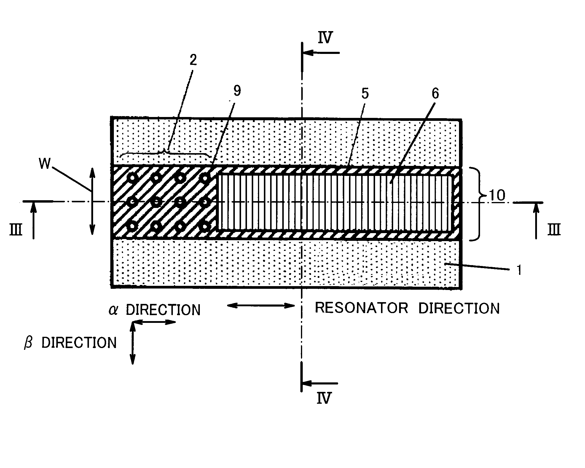
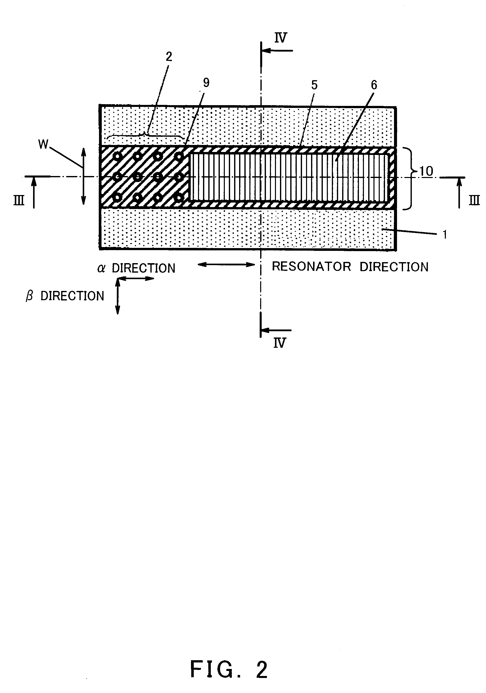
[0056] FIG. 2 is a plan view showing a structure of a semiconductor light emitting device according to the present invention. FIG. 3 is a view taken in the direction of arrows along line III-III in FIG. 2. FIG. 4 is a view taken in the direction of arrows along line IV-IV in FIG. 2. In this embodiment, a light emitting wavelength of the semiconductor light emitting device is set to 1.3 .mu.m.

[0057] As shown in FIGS. 2 to 4, a stripe structure 10 is provided on a n-type InP substrate 1. The stripe structure 10 has a n-type InP lower cladding layer 3 (100 nm thick), an InGaAsP / InGaAsP quantum well active layer 4 (hereinafter simply referred to as an active layer 4), and a p-type InP upper cladding layer 5 (50 nm thick), which are disposed in this order. The active layer 4 has a strained quantum well structure comprised of five pairs of In.sub.0.9Ga.sub.0.1As.sub.0.2P.sub.0.8 barrier layers (thickness: 10 nm, composition wavelength: 1.1 .mu.m, lattice strain: 0%), In.sub.0.9Ga.sub.0.1A...

embodiment 2

[0085] In a second embodiment, a description will be given of a semiconductor light emitting device configured to have photonic crystal as in the first embodiment and have a period of the photonic crystal in the resonator direction and a period of the photonic crystal in the direction perpendicular to the resonator direction which differ from each other.

[0086] FIG. 8 is a plan view showing a structure of a semiconductor light emitting device according to the second embodiment of the present invention. As shown in FIG. 8, the photonic crystal structure 2 is formed by arranging a plurality of concave portions 9 in the shape of rectangular lattice. Here, a period of the concave portions 9 in the resonator direction (spacing between adjacent concave portions 9) F1 is longer than a period F2 of the concave portions 9 in the direction perpendicular to the resonator direction. In FIG. 8, reference numeral 13 denotes a growth region where the p-type InP upper cladding layer is selectively g...

second embodiment

[0088] FIGS. 9A to 9D are views for explaining a method of fabricating the semiconductor light emitting device according to the present invention, FIG. 9A is a cross-sectional view showing a structure of the semiconductor light emitting device and FIGS. 9B to 9D are plan views showing a structure of the semiconductor light emitting device.

[0089] As shown in FIG. 9A, on the n-type InP substrate 1, the Si-doped n-type InP lower cladding layer 3 (100 nm thick), the undoped active layer 4 (14 nm thick), and the Zn-doped p-type InP upper cladding layer 5 (10 nm thick) are epitaxially grown by a known crystal growth method such as the MOVPE process. A SiO.sub.2 film 12 is formed on the p-type InP upper cladding layer 5.

[0090] Subsequently, as shown in FIG. 19B, using the SiO.sub.2 film 12 as a selective growth mask, the p-type InP upper cladding layer 5 (100 nm thick) is selectively grown, thereby forming a plurality of cylindrical concave portions 9 arranged in the shape of rectangular l...


PUM


Abstract

A semiconductor light emitting device of the present invention comprises a n-type InP substrate (1), and a stripe structure (10) formed in the stripe shape on the n-type InP substrate (1) and comprised of a n-type InP lower cladding layer (3), an active layer (4) having a resonator in a direction parallel to the n-type InP substrate (1), and a p-type InP upper cladding layer (5). The stripe structure (10) has a photonic crystal structure (2) with concave portions 9 arranged in rectangular lattice shape, and the direction in which the concave portions (9) of the photonic crystal structure (2) are arranged corresponds with a resonator direction. A stripe-shaped upper electrode (6) is formed on the stripe structure (10) to extend in the resonator direction. The semiconductor light emitting device of the present invention so structured is configured to radiate light in the direction perpendicular to the n-type InP substrate (1).

Description

[0001] This is a continuation application under 35 U.S.C.111(a) of pending prior International Application No. PCT / JP03 / 01285, filed on Feb.7, 2003.BACKGROUND OF THE INVENTION[0002] 1. Field of the Invention[0003] The present relates to a semiconductor light emitting device of a surface emitting type using photonic crystal grown on a substrate and a method of fabricating the same.[0004] 2. Description of the Related Art[0005] The conventional semiconductor light emitting devices using photonic crystal are disclosed in, for example, Japanese Laid-Open Patent Application Publication No. Hei. 11-330619, Japanese Laid-Open Patent Application Publication No. 2001-308457, Japanese Laid-Open Patent Application Publication No. 2001-9800 (U.S. patent Publication No. 2002 / 0109134 specification), Japanese Laid-Open Patent Application Publication No. Sho 63-205984 (U.S. Pat. No. 4,847,844 specification), and Japanese Laid-Open Patent Application Publication No. 2002-062554.[0006] Likewise, the ...

Claims


Application Information

Patent Timeline
IPC IPC(8): H01S5/028H01S5/10H01S5/12H01S5/18H01S5/187H01S5/22H01S5/40H01S5/42
CPCH01S5/028H01S5/105H01S5/42H01S5/187H01S5/2201H01S5/124H01S5/11
Inventor OTSUKA, NOBUYUKIYOSHII, SHIGEOYOKOGAWA, TOSHIYA
Owner PANASONIC CORP
Why Eureka
Try Eureka