
Eureka
For R&D, Eureka makes reading and utilizing patents & technical documents easy.
Eureka AIR
Designed for self-driven R&D workflows. Generate viable solutions, solve complex R&D challenges, empower your innovation with AI.

Eureka Materials
Designed for material experts only. Revolutionize your material R&D, from search, analyze, to developing new materials.

TechResearch
Generate reliable direction feasibility study reports for your R&D in just a few steps.

TechSeek
Discover and master advanced knowledge NOW. Basics, ideas, possibilities, all at once.

TechMind
As an expert in R&D Theories, TechMind can generates customized viable solutions instantly.

TechRisk
Analyze your overall solution with one click, know your potential R&D risks in advance.

TechMonitor
Get weekly tech updates, stay abreast of the latest tech innovations and key insights.
Reflective liquid crystal display device and fabricating method thereof
- Summary
- Abstract
- Description
- Claims
- Application Information
AI Technical Summary
Benefits of technology
Problems solved by technology
Method used
Image

Examples
Embodiment Construction
[0026] Reference will now be made in detail to the illustrated embodiments of the present invention, examples of which are illustrated in the accompanying drawings.
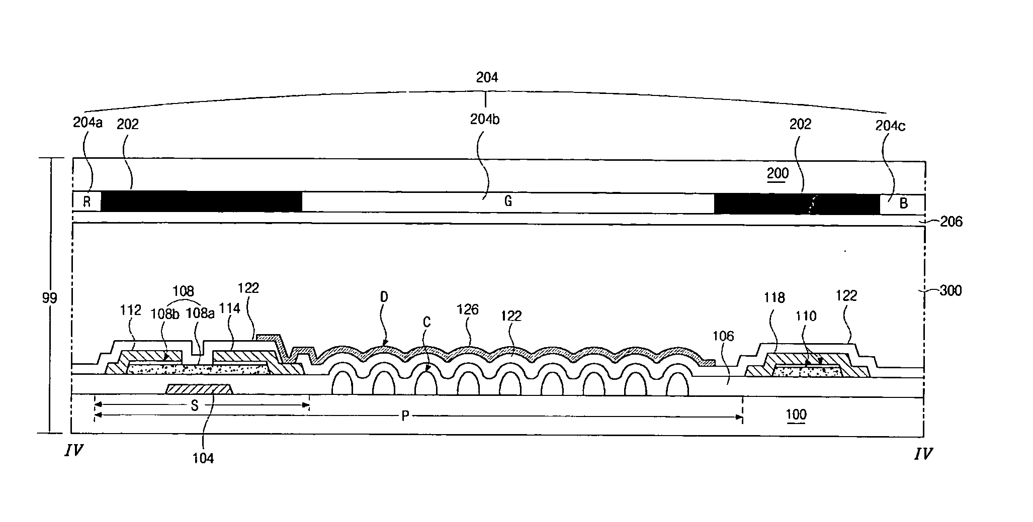
[0027] FIG. 3 is a schematic plane view of an array substrate for a reflective liquid crystal display device according to an embodiment of the present invention. In FIG. 3, a gate line 102 is formed on a substrate 100, and a data line 118 intersects the gate line 102 to define a pixel region "P." A thin film transistor (TFT) "T" including a gate electrode 104, a first semiconductor layer 108, a source electrode 114, and a drain electrode 116 is connected to the gate line 102 and the data line 118. A metal pattern 120 with an island shape is formed over the gate line 102. A storage capacitor "CSt" using a portion of the gate line 102 as a first electrode and the metal pattern 120 as a second electrode is formed at one side of the pixel region "P." A reflective layer 126 contacting the drain electrode 114 is formed in the p...
PUM
 Abstract
Description
Claims
Application Information
 - R&D Engineer
- R&D Manager
- IP Professional
- Industry Leading Data Capabilities
- Powerful AI technology
- Patent DNA Extraction
Browse by: Latest US Patents, China's latest patents, Technical Efficacy Thesaurus, Application Domain, Technology Topic, Popular Technical Reports.
© 2024 PatSnap. All rights reserved.Legal|Privacy policy|Modern Slavery Act Transparency Statement|Sitemap|About US| Contact US: help@patsnap.com