Photo-coupler semiconductor device and production method therefor

a technology of photo-coupler and semiconductor, which is applied in the direction of semiconductor/solid-state device manufacturing, semiconductor devices, electrical apparatus, etc., can solve the problems of unstable shape of encapsulant, encapsulant is prone to cracking, and the method of potting the light emitting element and the light receiving element in the encapsulant is not suitable for mass production

Inactive Publication Date: 2004-08-05
SHARP KK
View PDF4 Cites 12 Cited by
  • Summary
  • Abstract
  • Description
  • Claims
  • Application Information

AI Technical Summary

Problems solved by technology

However, the silicone resin to be used for covering the light emitting element and the light receiving element to form a light transmission path has a high linear expansion coefficient, so that the resulting package is liable to crack due to a thermal stress occur

Method used


Image

  • Photo-coupler semiconductor device and production method therefor
  • Photo-coupler semiconductor device and production method therefor
  • Photo-coupler semiconductor device and production method therefor

Examples


first embodiment

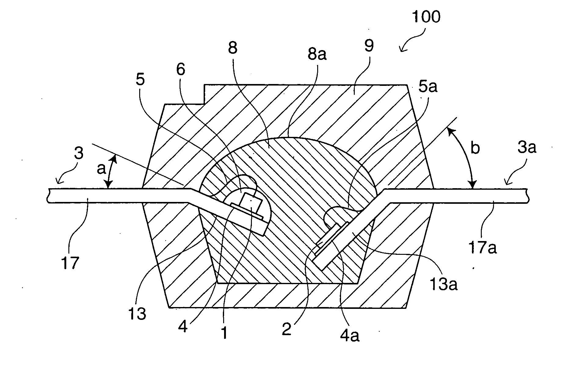
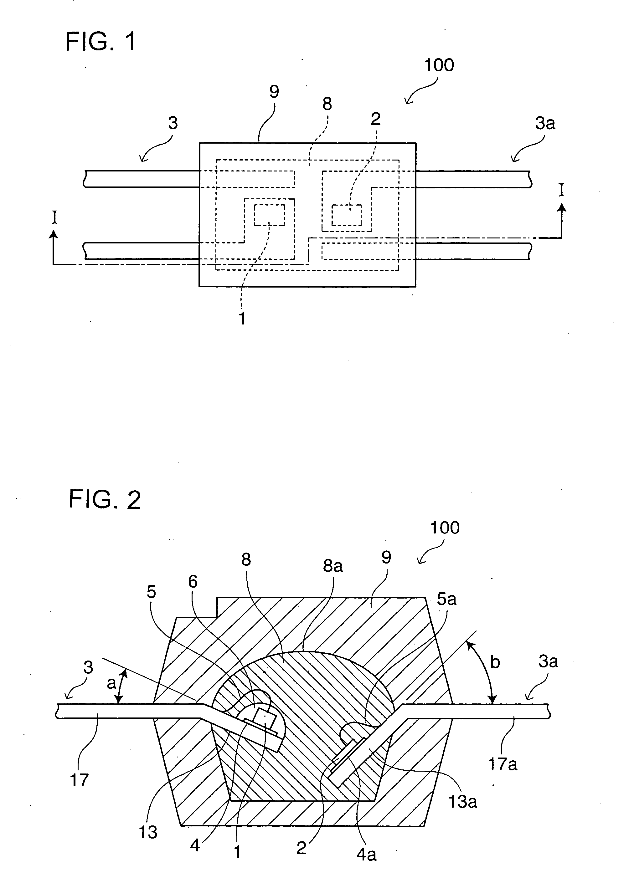
[0043] FIG. 1 is a plan view illustrating a photo-coupler semiconductor device (hereinafter referred to simply as "photo-coupler") according to the present invention, and FIG. 2 is a sectional view of the photo-coupler as seen in an arrow direction I-I in FIG. 1. As shown, the photo-coupler 100 includes a light emitting element 1 and a light receiving element 2 which are bonded to upper surfaces of distal portions 13 and 13a of first and second planar lead frames 3 and 3a by silver paste portions 4 and 4a, respectively, and are electrically connected (or wire-bonded) to the first and second lead frames 3 and 3a via gold wires 5 and 5a, respectively.

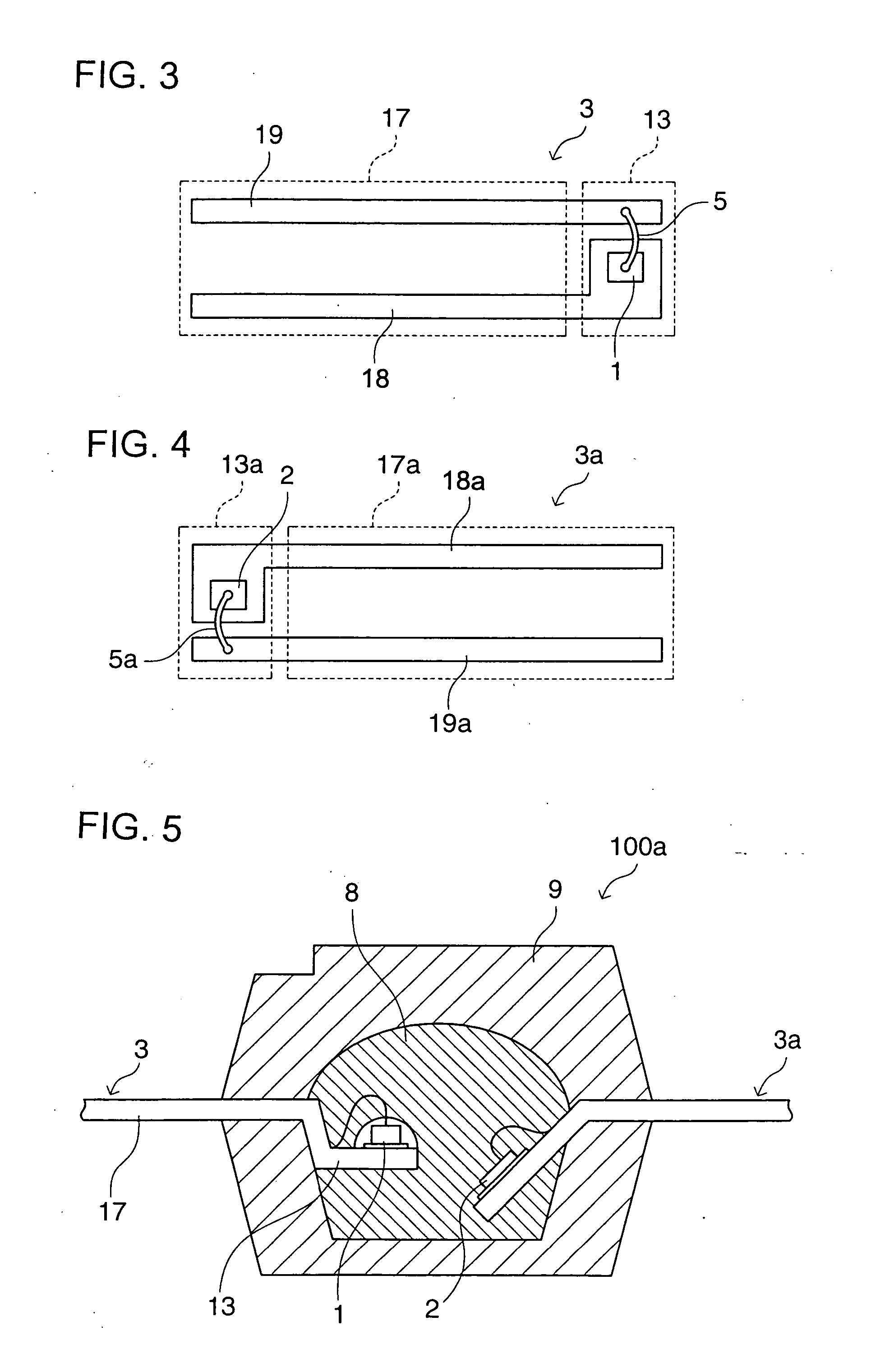
[0044] FIGS. 3 and 4 are plan views respectively illustrating the first and second lead frames 3 and 3a. As shown in FIG. 3, the first lead frame 3 has the distal portion 13 and a main portion 17, and is divided into an element mount frame 18 and a signal frame 19 which are arranged in parallel relation.

[0045] The light emitting element 1...

second embodiment

[0061] FIG. 11 is a diagram illustrating a photo-coupler according to a second embodiment of the present invention as corresponding to FIG. 2.

[0062] The photo-coupler 100b has substantially the same construction as the photo-coupler 100 shown in FIG. 2, except that the portion of the transparent resin member 8 above the light emitting element 1 and the light receiving element 2 has a generally truncated quadrangular pyramid shape and the upper surfaces of the distal portions 13, 13a of the first and second lead frames 3, 3a respectively form angles .alpha., .beta.of 45 to 90 degrees with respect to outer peripheral surface portions of the transparent resin member 8 adjacent thereto.

[0063] This arrangement makes it possible to produce the mold for the primary transfer molding at lower costs without the need for special processing which is otherwise required for mirror-finishing the hemispherical surface of the mold for the molding of the transparent resin member 8. Therefore, the cos...


PUM


Abstract

A photo-coupler semiconductor device includes first and second planar lead frames each having a main portion and a distal portion, a light emitting element and a light receiving element respectively mounted on upper surfaces of the distal portions of the first and second lead frames, a light-transmitting resin member which covers the light emitting element and the light receiving element, and supports the distal portions of the first and second lead frames in spaced opposed relation with the light emitting element and the light receiving element being mounted on the upper surfaces of the distal portions so that the main portions of the first and second lead frames are located in coplanar relation, and a opaque resin member which covers the light-transmitting resin member, and supports the main portions of the first and second lead frames. The light-transmitting resin member and the opaque resin member are each composed of an epoxy resin as a base resin.

Description

[0001] This application is related to Japanese patent application Nos.2003-009991 (filed on Jan. 17, 2003) and 2003-321627 (filed on Sep. 12, 2003), whose priorities are claimed under 35 USC .sctn. 119, the disclosures of which are incorporated by reference in their entirety.[0002] 1. Field of the Invention[0003] The present invention relates to a photo-coupler semiconductor device (photo-coupler) and to a production method therefor.[0004] 2. Description of the Related Art[0005] Japanese Unexamined Patent Publication No. Hei 11-177124 (1999), for example, discloses a prior-art photo-coupler related to the present invention, which is designed so that light emitted from a light emitting element is received by a light receiving element. The light emitting element and the light receiving element are located in opposed relation on die pads of first and second lead frames, respectively, which are inclined with respect to each other, and encapsulated in an encapsulant of a light-transmitti...

Claims


Application Information

Patent Timeline
IPC IPC(8): H01L31/12H01L25/16H01L31/16
CPCH01L25/167H01L31/16H01L2924/3025H01L2224/73265H01L2224/48247H01L2224/48091H01L2224/32245H01L2224/32013H01L2224/45144H01L2924/00014H01L2924/00H01L2924/181H01L2924/00012
Inventor SHOJI, HIROYUKITAKAKURA, HIDEYAKUSUDA, KAZUO
Owner SHARP KK
Why Eureka
Try Eureka