First and second level packaging assemblies and method of assembling package

a technology of packaging and assembly, applied in the direction of semiconductor devices, semiconductor/solid-state device details, electrical apparatus, etc., can solve the problems of weak mechanical strength of materials used in recent electronic devices, lead outflow from electronic products dumped on reclaimed land, pollute rivers and underground water,

Inactive Publication Date: 2004-08-12
KK TOSHIBA
View PDF8 Cites 77 Cited by
  • Summary
  • Abstract
  • Description
  • Claims
  • Application Information

AI Technical Summary

Problems solved by technology

However, recently, it has been pointed out that the outflow of lead from electronic products dumped onto reclaimed land pollutes rivers and underground water.
Meanwhile, since recent microprocessors process huge quantities of information at high speed, there have been problems with the resistance of wires interconnecting transistors, and the capacitance of insulators between interconnect wires.
However, such materials used in recent electronic devices are generally weak in mechanical strength.
In particular, low-k films used as insulators within s

Method used


Image

  • First and second level packaging assemblies and method of assembling package
  • First and second level packaging assemblies and method of assembling package
  • First and second level packaging assemblies and method of assembling package

Examples


first embodiment

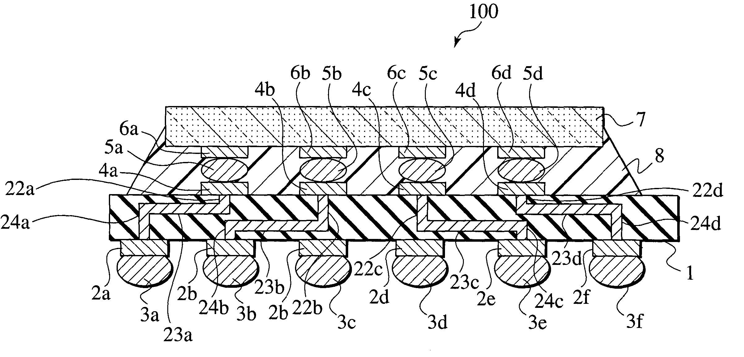
[0024] The first level packaging assembly 100 according to the present invention encompasses, as shown in FIG. 1: a chip-mounting base 1 defined by a first surface and a second surface opposite to the first surface; a plurality of solder balls 3a, 3b, 3c, 3d, 3e, and 3f connected to the first surface; a plurality of solder joints 5a, 5b, 5c, and 5d connected to the second surface including solder materials having a lower melting temperature than the solder balls; a semiconductor chip 7 defined by a third surface and a fourth surface opposite to the third surface, being connected to the solder joints 5a, 5b, 5c, and 5d on the second surface; and an underfill resin 8 sandwiched between the second and third surfaces so as to surround and encapsulate the solder joints.

[0025] On the third surface of the semiconductor chip 7, circuit elements 10 as shown in FIG. 3A are formed. In FIG. 1, the circuit elements (conductive layer) 10 and a protective film (passivation layer) 11 are omitted. A...

second embodiment

[0039] As shown in FIG. 5, a first assembly 101 according to a second embodiment of the present invention is different from the first assembly 100 shown in FIG. 1 in that solder joints 5a, 5b, 5c, and 5d disposed between a second surface of a chip-mounting base 1 and a third surface of a semiconductor chip 7 have lower melting temperature solder bumps (a first group) 18a, 18b, 18c, and 18d and higher melting temperature solder balls (a second group) 17a, 17b, 17c, and 17d. The lower melting temperature solder bumps 18a, 18b, 18c, and 18d have a lower melting temperature than Tin-Lead solder alloys. The higher melting temperature solder balls 17a, 17b, 17c, and 17d have a higher melting temperature than the lower melting temperature solder bumps 18a, 18b, 18c, and 18d.

[0040] The lower melting temperature solder bumps 18a, 18b, 18c, and 18d may have spherical shapes practically similar to those of the higher melting temperature solder balls 17a, 17b, 17c, and 17d. Moreover, the higher...

third embodiment

[0048] As shown in FIG. 8, a first assembly 102 according to a third embodiment of the present invention is different from the first assembly 100 shown in FIG. 1 in that a heat sink 19 is disposed on the second surface so as to surround the semiconductor chip 7. The heat sink 19 has a box shape having a square hollow space therein. The semiconductor chip 7 is disposed in the hollow space. The underfill resin 20 is disposed between the fourth surface of the semiconductor chip 7 and the hollow space of the heat sink 19. The heat sink 19 can be made from aluminum plate or the like.

[0049] Next, an assembly method of the first assembly 102 according to the third embodiment of the present invention is described. Since the method of assembling The first level packaging assembly 102 before attaching the heat sink 19 is the same shown in FIGS. 3A to 4B, a detailed explanation is omitted.

[0050] As shown in FIG. 9A, the heat sink 19 and a surface of the semiconductor chip 7 are opposed to each...


PUM


Abstract

A first level packaging assembly includes a chip-mounting base defined by a first surface and a second surface opposite to the first surface; a plurality of external connection lands disposed on the first surface; a plurality of solder balls connected to the external connection lands; a plurality of internal connection lands disposed on the second surface; a plurality of solder joints connected to the internal connection lands including solder materials having lower melting temperature than the solder balls; a semiconductor chip defined by a third surface and a fourth surface opposite to the third surface, connected to the solder joints on the third surface; and an underfill resin sandwiched between the second and third surfaces so as to mold the solder joints.

Description

[0001] This application is based upon and claims the benefit of priority from the prior Japanese Patent Applications No. P2003-030767, filed on Feb. 7, 2003; the entire contents of which are incorporated herein by reference.[0002] 1. Field of the Invention[0003] The present invention relates to semiconductor device technology, more specifically to first and second level packaging assemblies and a method of assembling package using soldering technology.[0004] 2. Description of the Related Art[0005] Semiconductor integrated circuits such as LSI have achieved higher levels of integration in recent years. Semiconductor devices themselves are shrinking in geometry size, growing in the degree of on-chip integration, and their pin-counts are increasing. In view of assembling technology for a semiconductor device, a surface-mount package (SMP) has been commonly employed in addition to a conventional lead-insertion type package. As for the SMP, for example, a ball grid array (BGA) and a chip...

Claims


Application Information

Patent Timeline
IPC IPC(8): H01L21/52H01L23/12H01L21/56H01L21/60H01L23/36H01L23/488H01L23/498
CPCH01L21/563H01L23/36H01L23/488H01L23/49816H01L24/81H01L2224/13147H01L2224/16225H01L2224/73203H01L2224/73204H01L2224/73253H01L2224/81193H01L2224/81801H01L2224/83102H01L2224/92125H01L2924/01005H01L2924/01013H01L2924/01029H01L2924/0103H01L2924/01042H01L2924/01047H01L2924/01049H01L2924/0105H01L2924/01051H01L2924/01074H01L2924/01078H01L2924/01079H01L2924/01082H01L2924/01322H01L2924/09701H01L2924/14H01L2924/15174H01L2924/15311H01L2924/16152H01L2924/19041H01L2924/20104H01L2924/20105H01L2924/20106H01L2924/30105H01L2924/01006H01L2924/01019H01L2924/01033H01L2924/014H01L2924/0132H01L24/29H01L2224/32225H01L2224/29109H01L2224/29111H01L2924/0133H01L2924/1517H01L2924/157H01L2924/15787H01L2224/2919H01L2224/16235H01L2924/00H01L2924/01014H01L2924/01028H01L2924/01083H01L2224/13111H01L2924/00014H01L2224/13109H01L2924/0665H01L2924/351H01L2224/05571H01L2224/05573H01L2224/05568H01L2224/81011H01L2224/05624H01L2224/05644H01L2224/05647H01L23/12H01L21/52
Inventor IIJIMA, TOSHITSUNE
Owner KK TOSHIBA
Why Eureka
Try Eureka