Inspecting an array of electronic components

a technology of electronic components and arrays, applied in the direction of instruments, ways, images, etc., can solve the problems of affecting the performance of ic packages, unsatisfactory, and more difficult to handle,

Inactive Publication Date: 2004-08-12
ASM ASSEMBLY AUTOMATION LTD
View PDF14 Cites 75 Cited by
  • Summary
  • Abstract
  • Description
  • Claims
  • Application Information

AI Technical Summary

Problems solved by technology

Defects may affect the performance of the IC packages.
Such inspection may be performed by a human operator physically checking the packages for defects, but that is not ideal.
However, there are a number of problems with such an approach.
Since the IC packages have already been singulated, they are more difficult to handle.
With the ever-decreasing size of IC packages, the level of difficulty is increased.
This method is more efficient and cost-effective, especially since IC packages are gett

Method used


Image

  • Inspecting an array of electronic components
  • Inspecting an array of electronic components
  • Inspecting an array of electronic components

Examples


Embodiment Construction

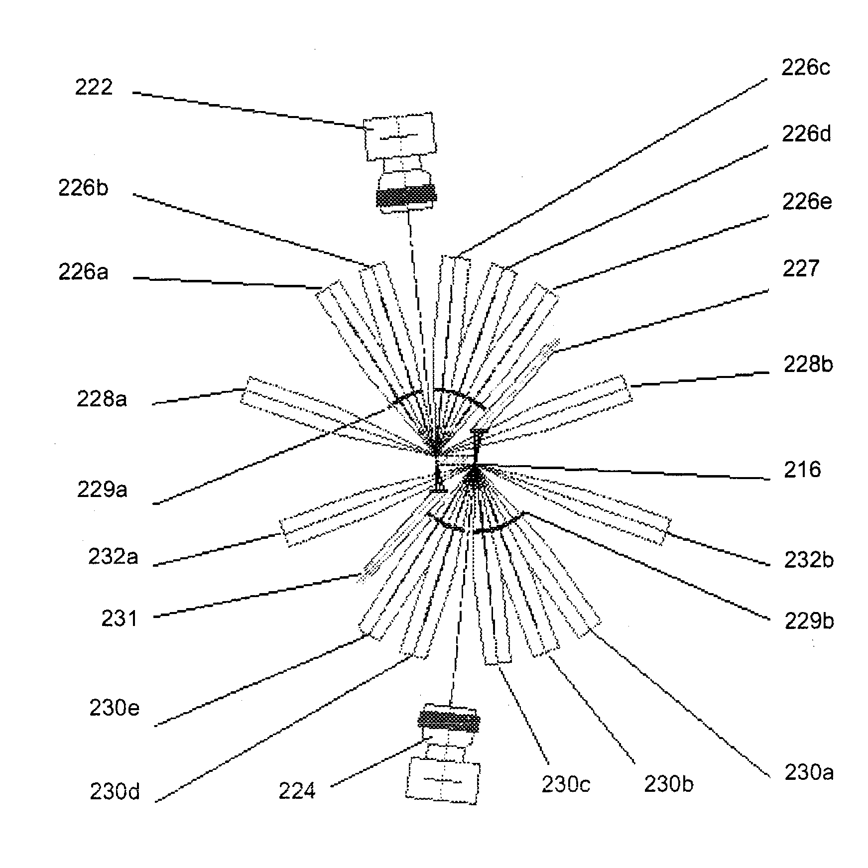
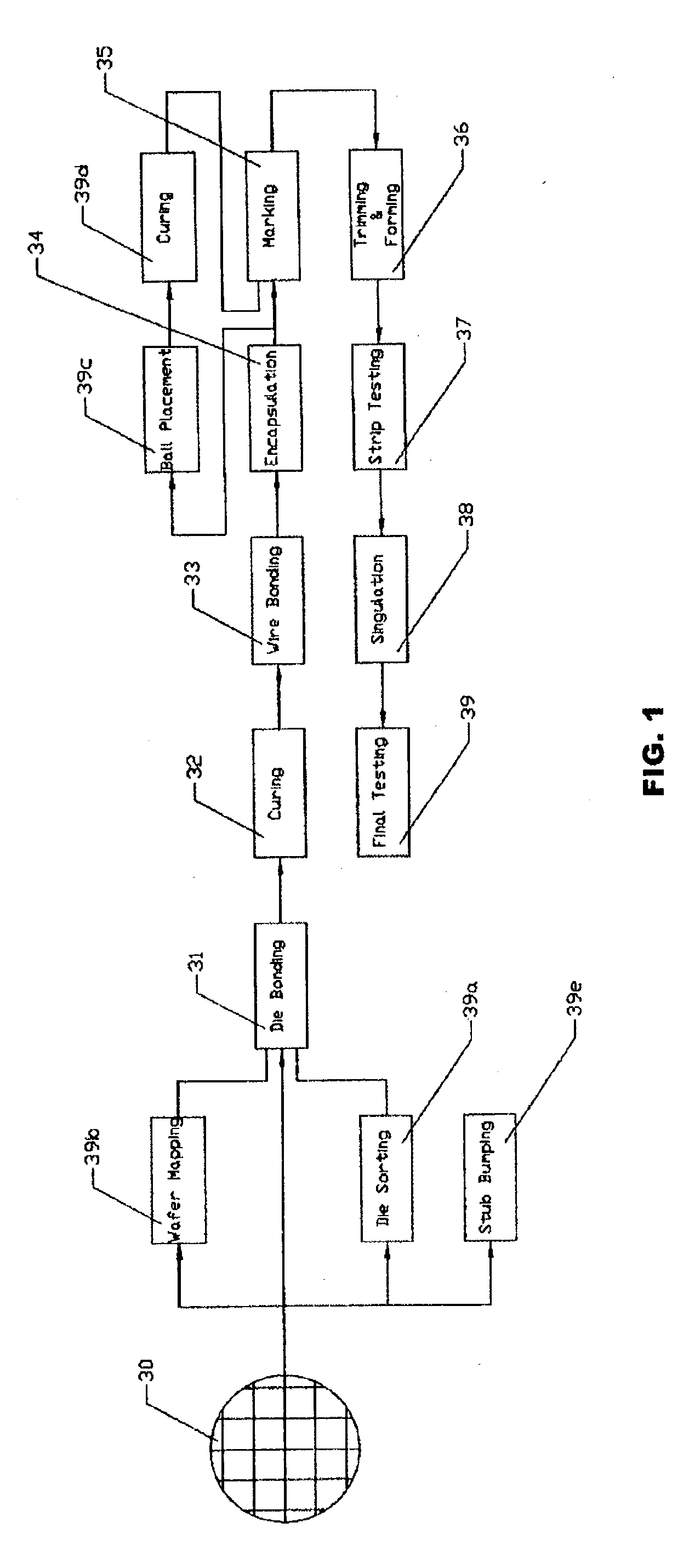
[0027] FIG. 1 shows a typical back-end Packaging Process Flow for micro-electronic components such as IC (Integrated Circuit) and LED (Light Emitting Diode) devices. Note that the process flow described is exemplary, and therefore some steps may be omitted or added, or combined or split, in other implementations. Actual implementation may also deviate from the flow depending on the property of the substrate, die and package type:

[0028] a. Semiconductor dice to be used in electronic packages are typically transported in the form of a wafer 30.

[0029] b. Prior to attaching a semiconductor die to a substrate in a Die Bonding Process 31, dice may be electrically, optically and visually tested for classification and grade sorting and transferred to different containers in accordance with their grade classification in a Die Sorting Process 39a. Then, containers with the same grade of die will be input to the die bonder for the Die Bonding Process 31. The Die Sorting Process 39a will ensure...


PUM

PropertyMeasurementUnit
Areaaaaaaaaaaa

Abstract

The invention provides an apparatus and method for inspecting an array of electronic components. The apparatus comprises a scanning device adapted to capture images of at least one surface of each of the respective components, whereby to inspect said surface. The scanning device may be a line scanning device.

Description

[0001] This invention relates to a method and apparatus for inspecting electronic components, such as semiconductor substrates with integrated circuits ("ICs") attached thereon, and in particular, to an automated inspection apparatus using scanning techniques. Such electronic components include, without limitation, semiconductor dice and leadframe packages that are involved in the packaging of a semiconductor IC package.BACKGROUND AND PRIOR ART[0002] In a typical packaging process of IC packages, such as Quad Flatpack No-lead ("QFN") or Ball-Grid Array ("BGA") packages, a plurality of encapsulated IC packages are usually formed on a single strip of substrate. These individual packages are then separated in a singulation process. Prior to or after singulation, the encapsulated packages on the substrates should be inspected to detect structural and other faults, such as lead coplanarity (for leaded packages) and defects in formation of a molded compound. Defects may affect the perform...

Claims


Application Information

Patent Timeline
IPC IPC(8): G01R31/26G01N21/89G01N21/956G06T7/00H01L21/60H01L21/66
CPCG01N21/8903G01N21/95684G06T7/0002G06T7/001G06T7/0022H01L2924/0002G06T2207/30148H01L2924/00G06T7/97E01C5/226E01C15/00E01C2201/165
Inventor JANSSON, DAVID ANDERSLEUNG, WING HONGCHEN, XU QIONG
Owner ASM ASSEMBLY AUTOMATION LTD
Why Eureka
Try Eureka