
Semiconductor device and method of manufacturing the same

a semiconductor device and semiconductor technology, applied in the direction of semiconductor devices, semiconductor/solid-state device testing/measurement, capacitors, etc., can solve the problems of limiting the degree to which the integration of the semiconductor device may be increased, and the cub structure tends to limit the degree of semiconductor device integration

Active Publication Date: 2004-09-09
SAMSUNG ELECTRONICS CO LTD
View PDF3 Cites 38 Cited by
  • Summary
  • Abstract
  • Description
  • Claims
  • Application Information

AI Technical Summary

Problems solved by technology

A disadvantage of the COB structure is that the cost of semiconductor fabrication is increased by the additional photolithographic processes, typically eight to ten, that may be required to add a COB structure to a standard logic device fabrication process.
On the other hand, the use of a CUB structure tends to limit the degree to which the integration of the semiconductor device may be increased.

Method used


Image

  • Semiconductor device and method of manufacturing the same
  • Semiconductor device and method of manufacturing the same
  • Semiconductor device and method of manufacturing the same

Examples


Embodiment Construction

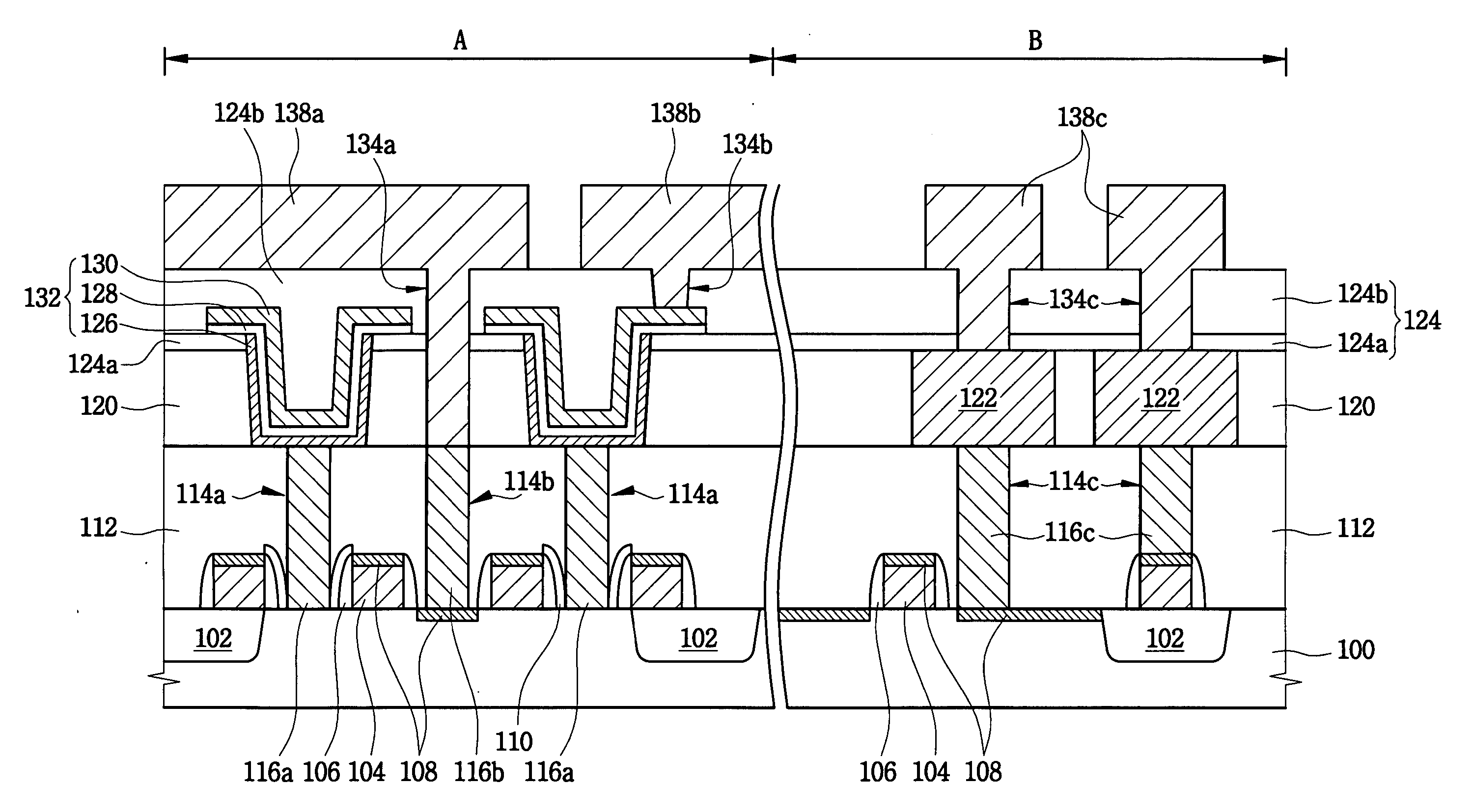
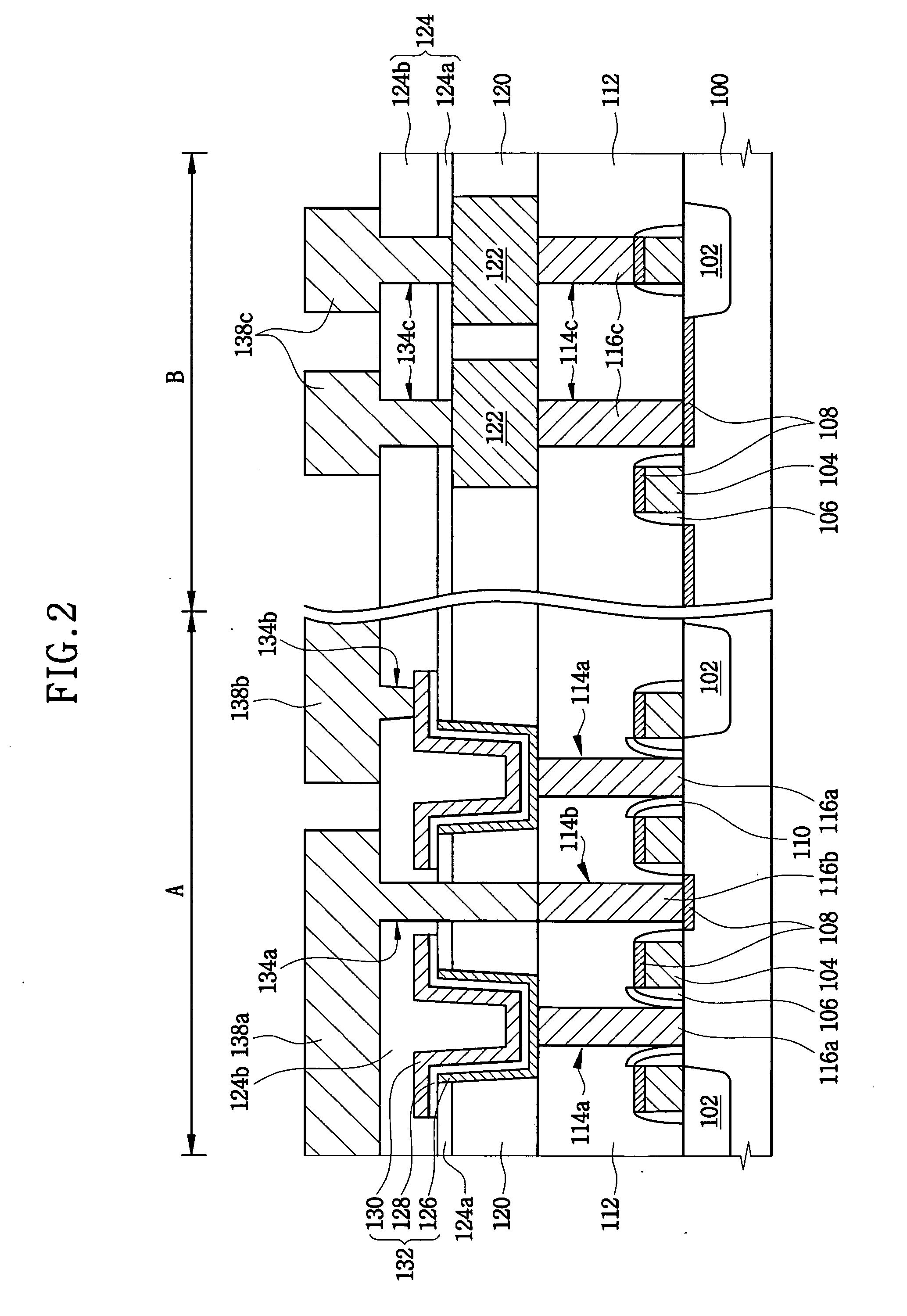
[0029] FIG. 2 is a cross sectional view illustrating an EDRAM device having a CUB structure according to an exemplary embodiment of the present invention.

[0030] Referring to FIG. 2, a substrate 100 is divided into a first region A and a second region B. The first region A corresponds to a cell array region, and the second region B corresponds to a core / peripheral circuit / logic region. Field regions separating and defining the active regions on the substrate 100 may be formed using conventional isolation techniques such as shallow trench isolation (STI).

[0031] MOS transistors are then formed on the first and second regions A and B of the substrate 100. The MOS transistors include first and second gate structures, each of which includes a gate electrode 104 and a gate spacer 106 formed on the sidewall of the gate electrode 104, a gate oxide layer (not shown), and an impurity region (not shown). The gate electrode 104 may include polysilicon doped with one or more impurities and the ga...


PUM


Abstract

Provided are semiconductor devices having a system-on-chip (SOC) configuration that combines both a capacitor-based cell-array memory region and one or more MOS core / peripheral circuit / logic regions on a single chip and a method for manufacturing such devices. The manufacturing process reduces the number of additional photolithographic processes required and modifies the relationship between the sizing of various layers and / or structures to reduce the fabrication cost and improve the reliability of the resulting devices. In particular, the capacitors for the memory region are formed in the same insulating layer as the first metal pattern for the core / peripheral circuit / logic regions of the devices, thereby producing capacitors and metal patterns of substantially the same height and thickness respectively. A landing structure may also be formed in the cell array region in combination with the first metal pattern for improving the contact process in the cell array region.

Description

[0001] This application claims priority under 35 USC .sctn. 119 to Korean Patent Application No. 2003-14414, filed on Mar. 7, 2003, the contents of which are herein incorporated by reference in their entirety for all purposes.[0002] 1. Field of the Invention[0003] The present invention relates to a semiconductor device and a method of manufacturing the same and, more particularly, to an embedded dynamic random access memory (EDRAM) having a capacitor-under-bitline (CUB) structure and a method of manufacturing such an EDRAM.[0004] 2. Description of the Related Art[0005] As semiconductor devices have become more highly integrated, a system on a chip (SOC) technology has become more widely employed in semiconductor fabricating processes. The SOC technology provides value added features to the semiconductor device by integrating elements having various functions in single chip, thus reducing the number of chips required and the assembly complexity and potentially improving the speed and...

Claims


Application Information

Patent Timeline
IPC IPC(8): H01L21/02H01L21/8242H01L21/316H01L21/66H01L27/108
CPCH01L21/31691H01L27/10811H01L28/65H01L27/10894H01L28/55H01L27/10885H10B12/312H10B12/09H10B12/482H10B12/00
Inventor OH, JAE-HEELEE, DUCK-HYUNG
Owner SAMSUNG ELECTRONICS CO LTD
Learn More