Display panel and electronic apparatus with the same
- Summary
- Abstract
- Description
- Claims
- Application Information
AI Technical Summary
Benefits of technology
Problems solved by technology
Method used
Image

Examples
first embodiment
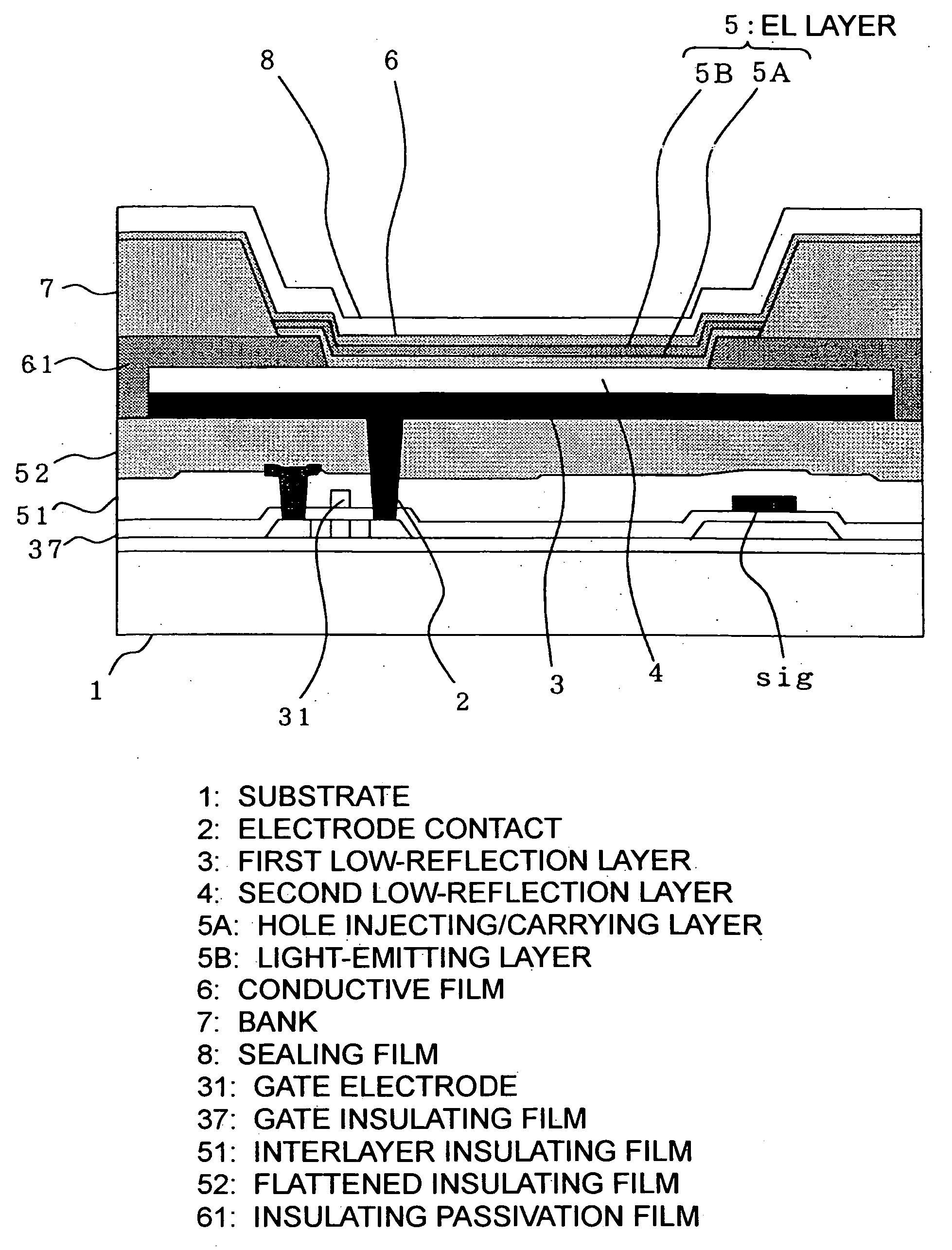
[0064] FIG. 1 is a partial cross-sectional view showing a structure of a display panel according to a first embodiment of the present invention. In FIG. 1, reference numerall indicates a substrate. In this embodiment, the substrate 1 is provided with a semiconductor film having a thin film transistor (hereinafter, referred to as TFT) serving as a control element (driving element).
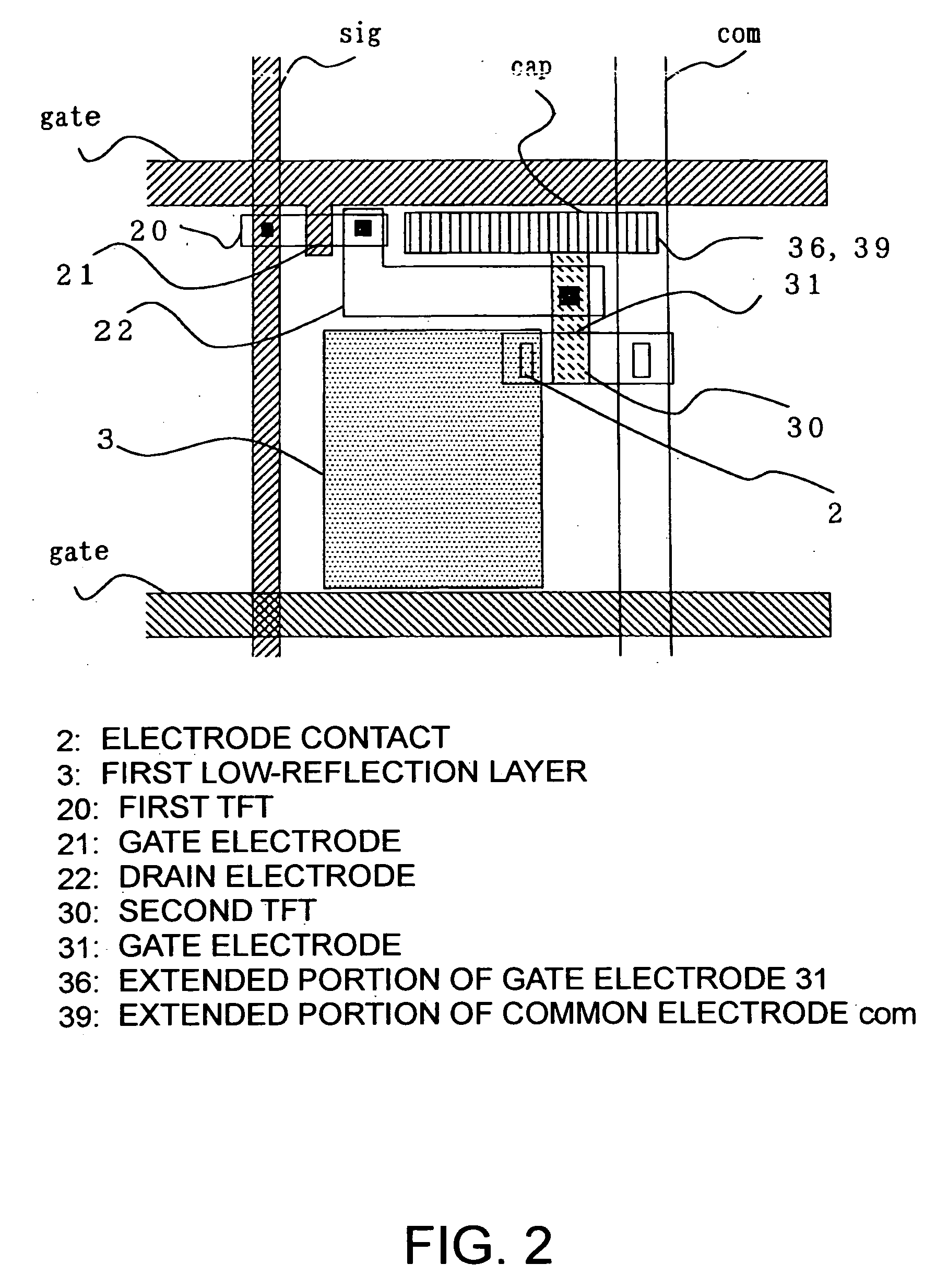
[0065] FIG. 2 is a plan view showing one pixel that constitutes the display panel. FIG. 2 shows elements formed on the substrate and positioned below a second low-reflection layer 4 shown in FIG. 1. A gate electrode 21 of a first TFT 20 is supplied with a scan signal via a scanning line "gate". A holding capacitor "cap" is adapted to hold an image signal supplied from a data line "sig" via the first TFT 20. A gate electrode 31 of a second TFT 30 is supplied with the image signal held by the holding capacitor "cap".
[0066] The first TFT 20 and the second TFT 30 are formed on an island-shaped semiconductor fil...
second embodiment
[0089] FIGS. 8 and 9 are partial cross-sectional views showing a construction of a display panel according to a second embodiment of the present invention. In the drawings, since elements indicated by the same reference numerals as those in FIG. 1 are the same or equivalent as those described in the first embodiment, the description thereof will be omitted herein. Instead of the sealing film 8 of the first embodiment, the second embodiment forms a low-reflection layer to reduce the reflectance of light incident from the exterior between the light-emitting layers by using a transparent sealing plate 8A such as a resin or glass functioning as a sealant, i.e., at a region of the sealing plate 8A opposite to the partition wall 7. Accordingly, in the second embodiment, it is not necessary to extend the low-reflection layer consisting of the first low-reflection layer 3 and the second low-reflection layer 4 to the bottom portion of the partition wall. Further, the low-reflection layer is ...
third embodiment
[0094] FIGS. 10 and 11 are partial cross-sectional views showing a construction of a display panel according to a third embodiment of the present invention. In the drawing, since elements indicated by the same reference numerals as those in FIG. 1 are the same or equivalent as those described in the first embodiment, the description thereof will be omitted herein. The third embodiment forms a low-reflection layer on the top face of the partition wall 7 for suppressing the light reflectance between the pixels. That is, instead of forming the low-reflection layer on the bottom portion of the partition wall or the sealant as shown in the first and second embodiments the low-reflection layer is formed on the surface of the partition wall 7. Accordingly, in the third embodiment, it is not necessary to extend the low-reflection layer consisting of the first low-reflection layer 3 and the second low-reflection layer 4 to the bottom portion of the partition wall. Further, the low reflection...
PUM
| Property | Measurement | Unit |
|---|---|---|
| Thickness | aaaaa | aaaaa |
| Thickness | aaaaa | aaaaa |
| Thickness | aaaaa | aaaaa |
Abstract
Description
Claims
Application Information
 - Generate Ideas
- Intellectual Property
- Life Sciences
- Materials
- Tech Scout
- Unparalleled Data Quality
- Higher Quality Content
- 60% Fewer Hallucinations
Browse by: Latest US Patents, China's latest patents, Technical Efficacy Thesaurus, Application Domain, Technology Topic, Popular Technical Reports.
© 2025 PatSnap. All rights reserved.Legal|Privacy policy|Modern Slavery Act Transparency Statement|Sitemap|About US| Contact US: help@patsnap.com