Compact low cost plastic MCM to PCB

a plastic multi-chip module and low-cost technology, applied in the direction of printed circuit aspects, printed circuit non-printed electric components association, electrical apparatus contruction details, etc., can solve the problems of inability to meet data transfer demands, system performance suffers, and the concept of arbitrating for a common bus shared across multiple boards is limiting in the more demanding applications

Inactive Publication Date: 2004-09-30
NORTHROP GRUMAN CORP
View PDF9 Cites 67 Cited by
  • Summary
  • Abstract
  • Description
  • Claims
  • Application Information

AI Technical Summary

Problems solved by technology

However, Integrated circuit (IC) technology and system infrastructures for connecting these devices to each other and to peripherals has not kept pace with the data transfer demands.
As a result, overall system performance often suffer

Method used


Image

  • Compact low cost plastic MCM to PCB
  • Compact low cost plastic MCM to PCB
  • Compact low cost plastic MCM to PCB

Examples


Embodiment Construction

[0031] The present invention is now described with reference to the drawings, wherein like reference numerals are used to refer to like elements throughout. In the following description, for purposes of explanation, numerous specific details are set forth in order to provide a thorough understanding of the present invention. It may be evident, however, that the present invention may be practiced without these specific details. In other instances, well-known structures and devices are shown in block diagram form in order to facilitate describing the present invention.

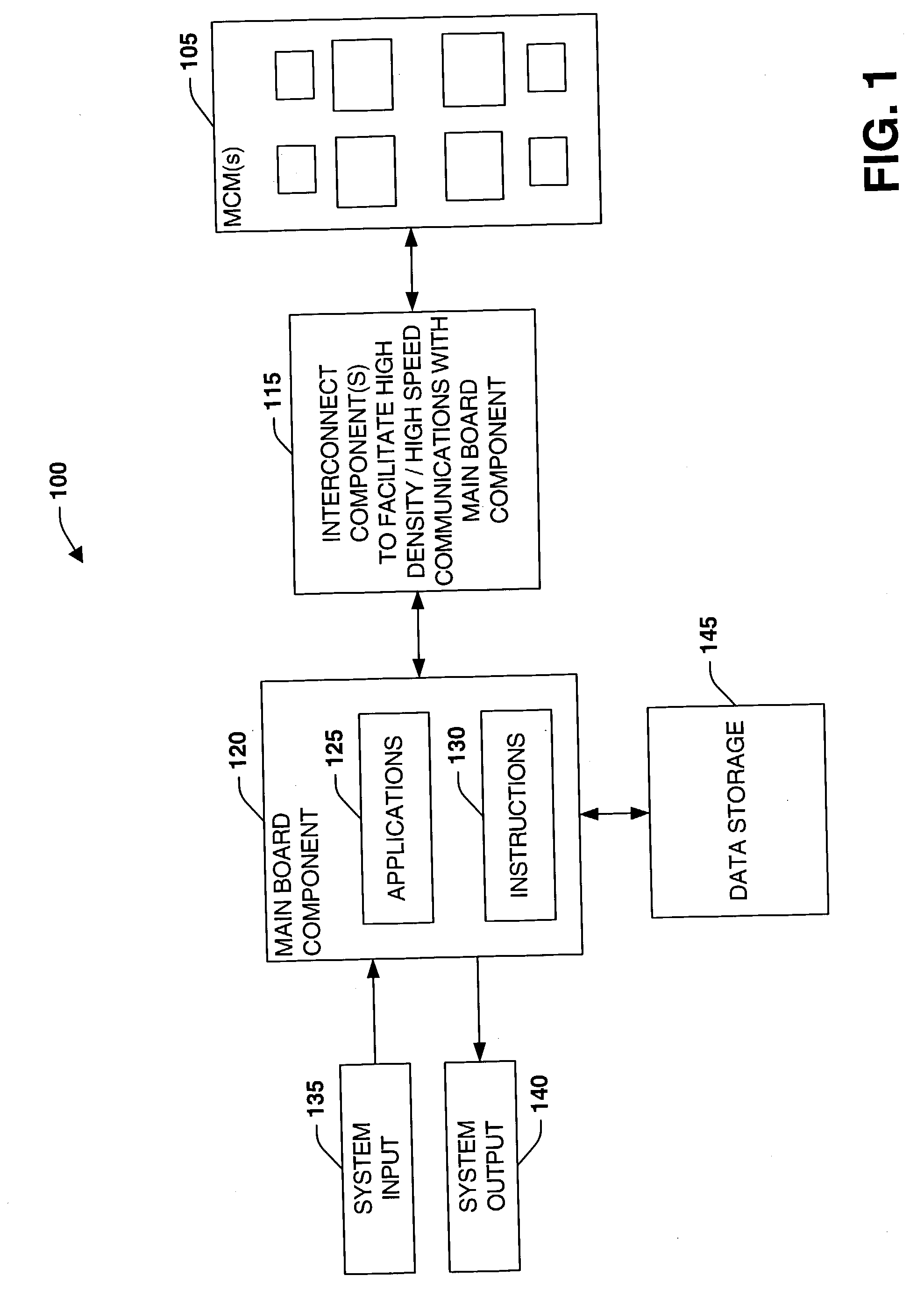
[0032] The subject invention relates to a system and methodology to reduce size, weight and cost, improve data processing rates, system scalability and serviceability and accommodate higher 10 integrated circuits (ICs) for printed circuit board (PCB) assemblies. This can be achieved by modularizing signal processing hardware and firmware on compact removable subunits or modules. Respective modules can be constructed with...


PUM


Abstract

The present invention relates to a system and methodology to reduce size, weight and cost, improve data processing rates and serviceability, and accommodate higher I/O multi-chip modules (MCMs) for printed circuit board (PCB) assemblies employed in the electronics industry. This is accomplished by selecting low cost, pre-assembled, plastic chip type MCMs for constructing a daughter card where the daughter card material can accommodate high density lines and spaces. Optical interconnects are employed between the daughter card and the motherboard to provide a high speed interface that is substantially not effected by contaminates or limitations associated with electrical lead wires and solder bonds. The result is a high performance card that meets current and projected future demands in signal processing.

Description

[0001] 1. Field of the Invention[0002] The present invention relates to a system and methodology for signal processing, and in particular to a compact, low cost, plastic multi-chip module (p-MCM) daughter board operatively coupled to a printed circuit board (PCB) for signal processing in the aerospace industry.[0003] 2. Discussion of the Related Art[0004] The evolution in electrical / electronical technologies has embedded signal processing with substantially every aspect of contemporary culture. Generally, any device that requires analog, digital and / or radio frequency (RF) signals to be processed employs signal processing. This marriage of signal processing and society has lead to breakthroughs and discoveries in areas dependent on information gathered through signal characteristics.[0005] Several examples of utilities that employ signal processing include personal computers (PCs), automobiles, cell phones, aircraft, satellite and spacecraft. Personal computers have become indispens...

Claims


Application Information

Patent Timeline
IPC IPC(8): G02B6/43H05K1/14H05K1/18
CPCG02B6/43H05K2201/10121H05K1/181H05K1/141H01L2224/48091H01L2224/48227H01L2224/73204H01L2924/15311H01L2924/00014
Inventor SAITO, YOSHIOESTES, THOMAS J.BERENZ, JOHN J.
Owner NORTHROP GRUMAN CORP
Why Eureka
Try Eureka