
SOI substrate and manufacturing method thereof

Inactive Publication Date: 2004-11-25
SUMITOMO MITSUBISHI SILICON CORP
View PDF0 Cites 2 Cited by
  • Summary
  • Abstract
  • Description
  • Claims
  • Application Information

AI Technical Summary

Benefits of technology

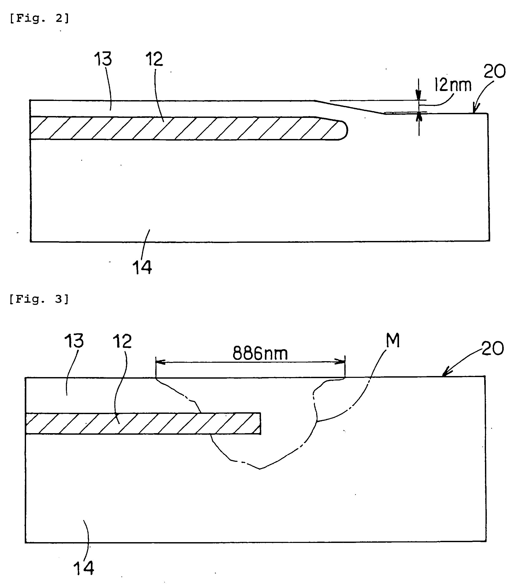
[0009] To this end, the inventors of the present invention have devoted themselves in an enthusiastic research and made the present invention based on the finding that if the thickness of a peripheral edge portion of a buried silicon oxide film formed partially in the SOI substrate is made thinner toward a terminal edge of the buried insulating film, an amount of expansion in volume of the buried silicon oxide film in the peripheral edge portion thereof during a high temperature thermal processing could be reduced decrementally or consecutively, to thereby reduce a strain / stress possibly induced in an interface between the buried silicon oxide film and a bulk layer and thus to inhibit said dislocation from being induced.
[0010] An object of the present invention is to provide an SOI substrate, in which a strain / stress possibly induced in an interface between a partially formed buried insulating film and a bulk layer can be reduced and thus the occurrence of a dislocation resultant from said strain / stress can be inhibited.
[0011] Another object of the present invention is to provide a manufacturing method of an SOI substrate that can inhibit the occurrence of dislocation of a partial SOI structure.
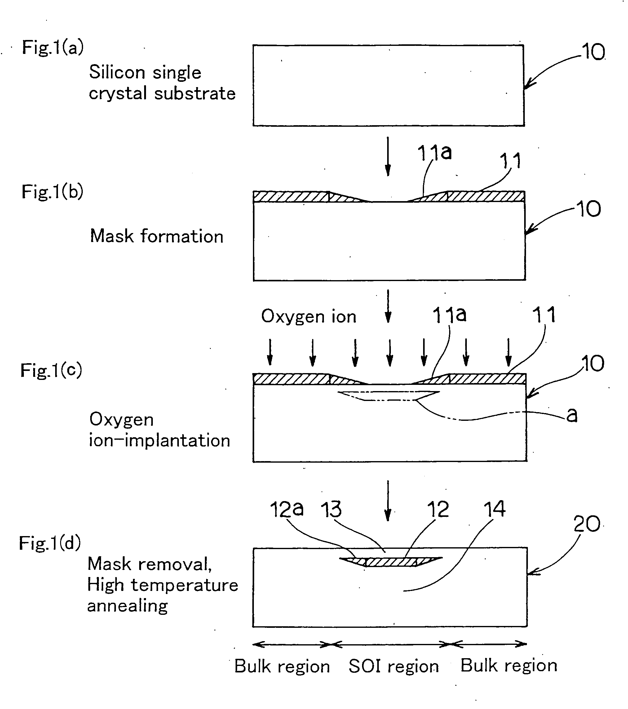
[0029] During the subsequent thermal processing, the fusion or bonding of the ion-implanted elements with the silicon is accelerated. Thus, the buried insulating film is formed partially in the silicon single crystal substrate. Therefore, within the silicon single crystal substrate, such a partial SOI structure consisting of the active layer, the buried insulating film and the bulk layer can be fabricated. During the formation of the buried insulating film in this thermal processing, the buried insulating film will be expanded in volume and induce the strain / stress in the interface between the buried silicon oxide film and the bulk layer. However, the amount of ion-implantation of the elements in the peripheral edge portion of the ion-implanted zone is getting lesser toward the terminal edge thereof. As a result, the induced strain / stress is relaxed in the peripheral edge portion having reduced thickness of the buried insulating film. Consequently, the strain / stress taking effect in the interface between the buried silicon oxide film and the bulk layer is reduced, thereby inhibiting the dislocation from being induced.
[0064] In the SOI substrate according to the present invention, since the thickness of the peripheral edge portion of the buried insulating film formed partially (in one part of its plane in plan view) in the interior of the silicon single crystal substrate has been made thinner toward the terminal edge of said buried insulating film, therefore the expansion in volume of the buried insulating film in said thinned film section during the thermal processing at high temperature can be reduced. This can help reduce the strain / stress in said thinned film section, which might be induced in the interface between the buried insulating film and the bulk layer, thus inhibiting the occurrence of the dislocation.
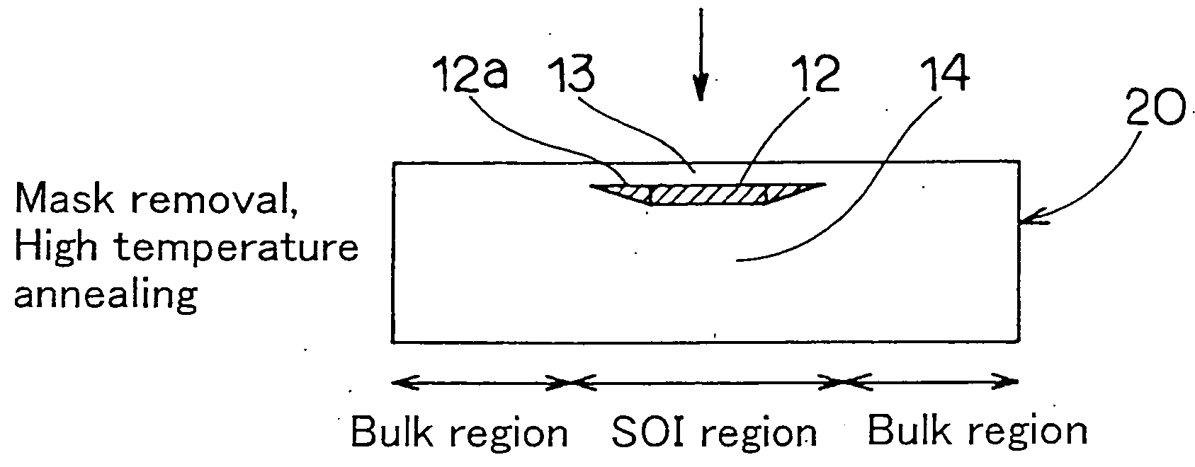
[0088] It is to be noted that during said high temperature annealing process, the strain / stress may be induced in the interface between each buried silicon oxide film 12 and the bulk layer 14 caused by an expansion in volume of the buried silicon oxide film 12, or a difference in the amount of expansion in volume between the silicon and the silicon oxide, within the silicon single crystal substrate 10. However, since the thickness of each buried silicon oxide film 12 in its peripheral edge portion 12a is getting gradually thinner toward the terminal end of the buried silicon oxide film 12 as described above, the strain / stress can be relaxed in the peripheral edge portion 12a of each buried silicon oxide film 12. Owing to this, the occurrence of the dislocation resultant from the strain / stress can be inhibited.

Problems solved by technology

In such a manufacturing method of the SIMOX substrate as stated above according to the prior art, however, the buried silicon oxide film is expanded in its volume during the high temperature thermal processing, leading to a strain / stress to be induced in an interface between the buried silicon oxide film and the bulk layer.
There is another fear remaining that if the pattern of the partial SOI structure became highly micro-fabricated in future, the dislocation of the pattern could affect inversely to yield of the device.

Method used


Image

  • SOI substrate and manufacturing method thereof
  • SOI substrate and manufacturing method thereof
  • SOI substrate and manufacturing method thereof

Examples


Embodiment Construction

1000 0 Test Example 2 about 500 0 Test Example 3 about 300 about 1.0 Test Example 4 about 200 about 1.5 Test Example 5 about 80 about 3.0 Test Example 6 about 10 about 7.5 Comparative 0 about 7.5 Example 1

[0097] It has been confirmed from Table 1 that as the width of the peripheral edge portion 12a of the buried silicon oxide film 12 is getting increased, the distance of propagation of the dislocation developed from the interface between the buried silicon oxide film 12 and the bulk layer 14 is getting shorter. It has been further confirmed that, for the case of the smaller width (shorter than 10 nm) of the peripheral edge portion 12a in the buried silicon oxide film 12, no inhibiting effect on the dislocation takes place. It has been also confirmed that in contrast to this, for the width of the thinning peripheral edge portion 12a over 1000 nm, almost no dislocation is induced.

[0098] Subsequently, with reference to FIG. 7 and FIG. 8, it has been confirmed by using the secondary ion...


PUM


Abstract

An SOI substrate having a partial SOI structure in which a buried insulating film having a predetermined area is formed via an active layer in a part of a silicon single crystal substrate in plan view by ion-implanting elements to the part of the substrate and then applying thereto a thermal processing, wherein a thickness of a peripheral edge portion of said buried insulating film is getting thinner toward a terminal edge of said buried insulating film.

Description

[0001] 1. Field of the Invention[0002] The present invention generally relates to an SOI (Silicon On Insulator) substrate and a manufacturing method thereof, and in particular, to an SOI substrate comprising a silicon substrate including in part an SOI structure in plan view, or an SOI substrate comprising a silicon substrate including in part a buried insulating film formed therein, and also to a manufacturing method thereof. Said SOI structure includes a SIMOX (Separation by IMplanted OXygen) structure.[0003] 2. Description of the Related Art[0004] Aiming for a reduction in a manufacturing cost of a device as well as an improvement of a working speed, the SoC (System on Chip) technology has been suggested for providing a mixed packaging of a logic circuit and a memory circuit on one chip. Preferably, this logic circuit may be fabricated on the SOI substrate in order to reduce electric power consumption and improve the working speed. Further, preferably the memory circuit may be fa...

Claims


Application Information

Patent Timeline
IPC IPC(8): H01L21/76H01L21/00H01L21/02H01L21/265H01L21/762H01L21/84H01L27/01H01L27/12
CPCH01L21/76243H01L21/84
Inventor AKATSUKA, MASANORIADACHI, NAOSHI
Owner SUMITOMO MITSUBISHI SILICON CORP
Learn More