Photovoltaic infrared radiation detector with independent three-dimensional conducting grid

Active Publication Date: 2004-12-02
COMMISSARIAT A LENERGIE ATOMIQUE ET AUX ENERGIES ALTERNATIVES
View PDF4 Cites 46 Cited by
  • Summary
  • Abstract
  • Description
  • Claims
  • Application Information

AI Technical Summary

Benefits of technology

0014] One object of the invention is to remedy these shortcomings and in particular to optimize the quantum

Problems solved by technology

Etching of the channels gives rise to several problems:
The channels between adjacent pixels being in general of non-negligible w

Method used


Image

  • Photovoltaic infrared radiation detector with independent three-dimensional conducting grid
  • Photovoltaic infrared radiation detector with independent three-dimensional conducting grid
  • Photovoltaic infrared radiation detector with independent three-dimensional conducting grid

Examples


Embodiment Construction

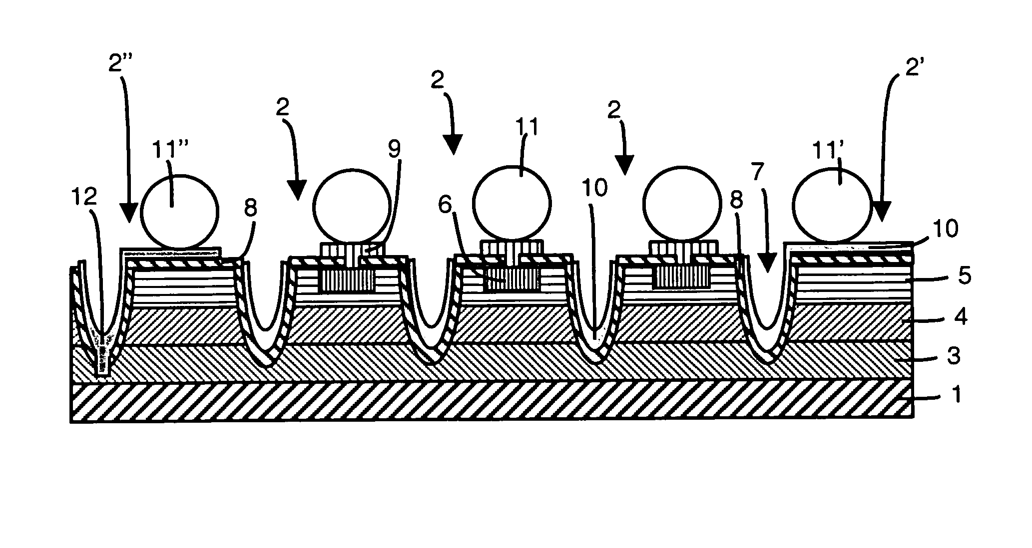
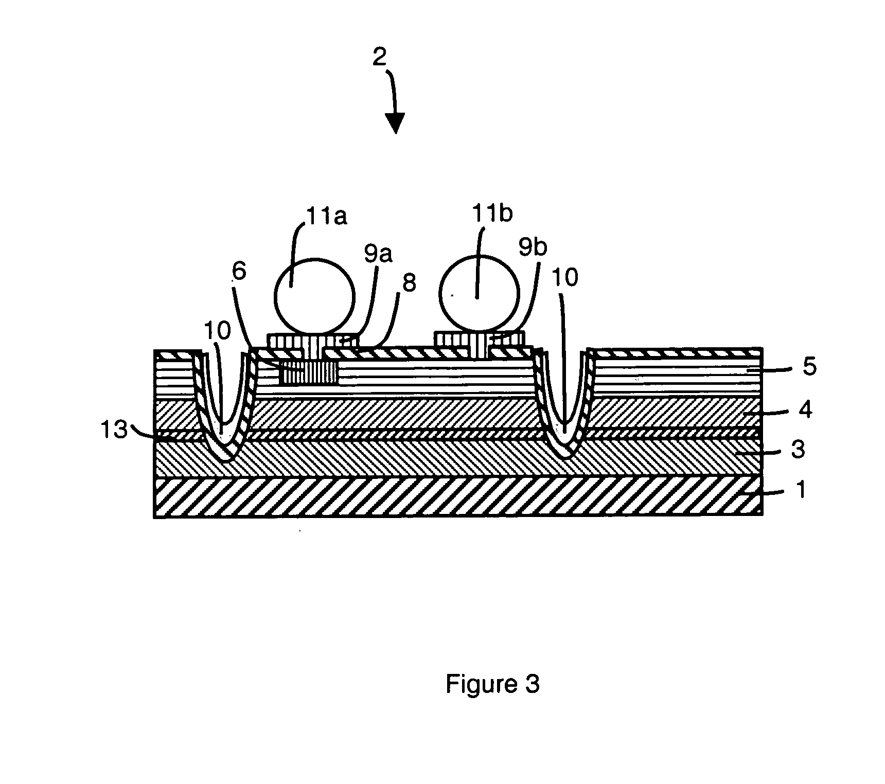
[0021] FIGS. 1 and 2 represent a photovoltaic infrared radiation detector enabling spatial coherence detection to be achieved. A network of active pixels 2 and inactive pixels (2', 2") is arranged on a front face of a substrate 1 transparent to the radiation considered. Each pixel is confined in a stack of layers 3-6 made of absorbent semi-conducting materials, and is separated from the adjacent pixels by substantially concave channels 7 made in the stack of layers 3-6 so as to form a network of communicating channels 7 perpendicular to one another (FIG. 2). The bottoms and side walls of the channels are covered with an insulating layer 8 that also covers the front face of the inactive pixels 2' and 2" arranged at the ends of the detector (to the left and to the right in FIGS. 1 and 2).

[0022] The front faces of the active pixels 2 are partially covered by the insulating layer 8 over a first peripheral zone of the front face leaving in the center of each active pixel 2 a second centr...


PUM


Abstract

On a front face of a substrate transparent to the radiation considered, pixels are confined in a stack of absorbent semi-conducting material layers by a network of channels. An insulating layer covers the bottom and the side walls of the channels. An electrically conducting layer covers the insulating layer on the bottom and on the side walls of the channels confining at least a part of the pixels. The conducting layer can be voltage polarized.

Description

[0001] The invention relates to a photovoltaic infrared radiation detector comprising, on a front face of a substrate transparent to the radiation considered, a stack of layers made of absorbent semi-conducting materials, a network of channels confining pixels in the stack of layers, and an insulating layer covering at least the bottom and side walls of the channels.STATE OF THE ART[0002] A semi-conductor-based multi-spectral photovoltaic infrared radiation detector is typically formed by a detection circuit and a read circuit:[0003] The detection circuit is made from a semi-conducting material absorbing radiation in one or more infrared bands of distinct cutoff wavelengths, and comprises photodiodes collecting the current from the photo-carriers generated.[0004] The read circuit performs multiplexing of the detection circuit photodiodes or interconnection of the detection circuit with an external circuit.[0005] The present invention concerns the detection circuit of such a detector...

Claims


Application Information

Patent Timeline
IPC IPC(8): H01L27/146
CPCH01L27/14649H01L27/14672
Inventor GRAVRAND, OLIVIERBAYLET, JACQUES
Owner COMMISSARIAT A LENERGIE ATOMIQUE ET AUX ENERGIES ALTERNATIVES
Why Eureka
Try Eureka