Dicing adhesive sheet and dicing method

a technology of adhesive sheet and dicing method, which is applied in the direction of film/foil adhesives, chemistry apparatus and processes, transportation and packaging, etc., can solve the problem of insufficient adhesion, and achieve the effect of effectively suppressing or preventing the cracking

Inactive Publication Date: 2005-01-06
NITTO DENKO CORP
View PDF0 Cites 13 Cited by
  • Summary
  • Abstract
  • Description
  • Claims
  • Application Information

AI Technical Summary

Benefits of technology

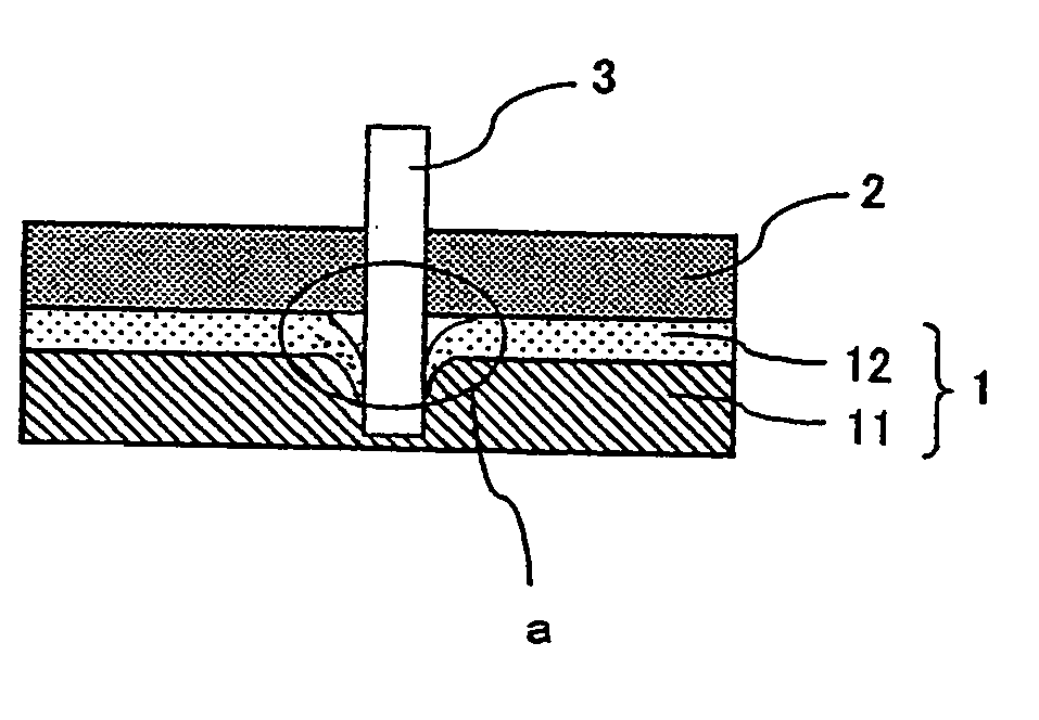
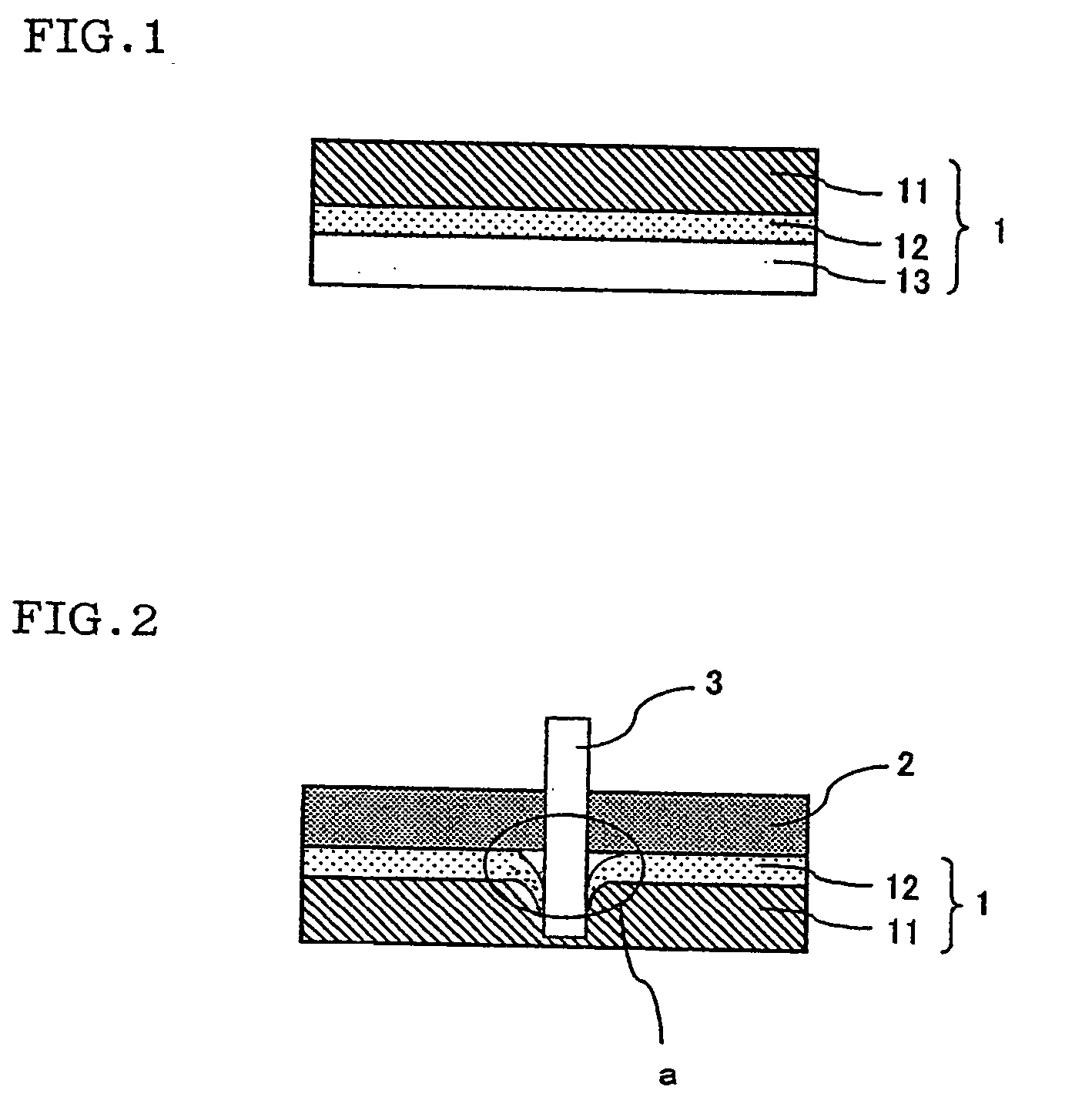
[0011] The dicing adhesive sheet according to this invention has a thin adhesive layer and exhibits a high peeling adhesion to the deiced body in the dicing process. Though the adhesive layer is vulnerable to deformation, such features can suppress or prevent deformation of the adhesive layer and suppress or prevent peeling at the interface between the chip and the adhesive layer, so that chipping is suppressed or prevented.
[0012] If the adhesive layer is too thin, the adhesion can tend to be insufficient. Therefore, the adhesive layer needs to have a thickness of 1 μm or more. From this viewpoint, the adhesive layer preferably has a thickness of 3 μm or more. On the other hand, if the adhesive layer is too thick, the rotation of the circular blade provide an increased amount of deformation of the whole adhesive layer, so that peeling can be facilitated at the interface between the semiconductor wafer and the adhesive layer both being cut with the blade. Therefore, the adhesive layer has a thickness of 10 μm or less. In this viewpoint, the adhesive layer preferably has a thickness of 7 μm or less. In particular, the adhesive layer preferably has a thickness of 3 to 7 μm.
[0013] The dicing adhesive sheet also exhibits a peeling adhesion such that the adhesion measured when 180° peeling (the peeling rate is 300 mm / min) at 23° C. of the dicing sheet is conducted after it is stuck to a silicon mirror wafer is 10 N / 25 mm or more. The adhesion is defined with respect to a silicon mirror wafer, because the silicon mirror wafer has a stable surface condition (roughness) and therefore is suitable as a general adherend and because such a silicon material can be the same as the material of a deiced body to be subjected to dicing. The adhesion is determined at 23° C. because dicing is generally performed at room temperature (23° C.). The adhesion of the dicing adhesive sheet to the silicon mirror wafer is 10 N / 25 mm or more, preferably 12 N / 25 mm or more. At a lower level of the adhesion, peeling can easily occur at the interface between the semiconductor wafer and the adhesive layer when the adhesive layer is deformed by the rotation of the circular blade during dicing.
[0019] The dicing adhesive sheet is stuck to the diced body at a temperature that will produce at least the above adhesion. The diced body is subjected to dicing while being fixed with the high peeling adhesion, so that chipping can effectively be suppressed or prevented by the dicing adhesive sheet.

Problems solved by technology

If the adhesive layer is too thin, the adhesion can tend to be insufficient.

Method used


Image

  • Dicing adhesive sheet and dicing method
  • Dicing adhesive sheet and dicing method

Examples


example 1

[0041] Base Film

[0042] The base film used was a linear low density polyethylene film with a thickness of 70 μm. One side of the film was corona treated.

[0043] Preparation of Adhesive

[0044] A solution of a radiation-curable acrylic adhesive was produced by adding 60 parts by weight of a radiation-curable oligomer (with a viscosity of 10 Pa·sec at 25° C.), 3 parts by weight of a photopolymerization initiator (Irgacure 651 (trade name) manufactured by Chiba Specialty Chemicals) and 2 parts by weight of a polyisocyanate compound (Coronate L (trade name) manufacture by Nippon Polyurethane Industry Co., Ltd.) to a solution containing an acrylic copolymer with a weight average molecular weight of 800,000. The radiation-curable oligomer was a product of the reaction of pentaerythritol triacrylate and diisocyanate. The acrylic copolymer was a product of conventional polymerization of 60 parts by weight of methyl acrylate (which can form a homopolymer with a Tg of 8° C.), 30 parts by weigh...

example 2

[0047] Preparation of Adhesive

[0048] A solution of a radiation-curable acrylic adhesive was produced by adding 50 parts by weight of pentaacrylate ester (Kayarad SR-9041 (trade name) manufactured by Nippon Kayaku Co., Ltd., with a viscosity of 15 Pa·sec at 25° C.), 3 parts by weight of a photopolymerization initiator (Irgacure 651 (trade name) manufactured by Chiba Specialty Chemicals) and 3 parts by weight of a polyisocyanate compound (Coronate L (trade name) manufacture by Nippon Polyurethane Industry Co., Ltd.) to a solution containing an acrylic copolymer with a weight average molecular weight of 700,000. The acrylic copolymer was a product of conventional polymerization of 50 parts by weight of ethyl acrylate (which can form a homopolymer with a Tg of −22° C.), 25 parts by weight of 2-ethylhexyl acrylate (which can form a homopolymer with a Tg of −85° C.), 20 parts by weight of acryloylmorpholine, and 5 parts by weight of acrylic acid (which can be form a homopolymer with a Tg...


PUM

PropertyMeasurementUnit
adhesionaaaaaaaaaa
thicknessaaaaaaaaaa
sticking temperatureaaaaaaaaaa

Abstract

A dicing adhesive sheet having a base film and an adhesive layer formed on the base film is characterized in that the thickness of the adhesive layer ranges from 1 to 10 μm and the adhesive layer has an sticking temperature such that the adhesion measured when 180° peeling at 23° C. of the dicing sheet is conducted (the peeling rate is 300 mm / min) after it is applied to a silicon mirror wafer is 10 N / 25 mm or more. In a dicing method using such a dicing adhesive sheet, the production yield of a diced body such as a semiconductor wafer is high, and chipping the dicing is prevented.

Description

TECHNICAL FIELD [0001] The present invention relates to a dicing adhesive sheet and to a dicing method using the dicing adhesive sheet. In particular, the dicing adhesive sheet of this invention is useful as a semiconductor wafer-dicing adhesive sheet, which is used to fix a deiced body such as a semiconductor wafer in the process of cutting and dividing (dicing) the semiconductor wafer or the like into device pieces. For example, the dicing adhesive sheet of this invention sheet can be used as a dicing adhesive sheet for in silicon semiconductor, a dicing adhesive sheet for compound semiconductor wafer, a dicing adhesive sheet for semiconductor package, a dicing adhesive sheet for glass, or the like. BACKGROUND ART [0002] Conventionally, a semiconductor wafer made of a material such as silicon, gallium, arsenic or the like is produced with its large diameter scale and then cut and divided (diced) into device pieces, which are then transferred to a mounting step. In such a process, ...

Claims


Application Information

Patent Timeline
Patent Type & Authority Applications(United States)
IPC IPC(8): C09J7/22C09J7/38H01L21/00H01L21/67H01L21/68H01L21/683
CPCC09J7/0217C09J7/0246C09J2203/326H01L21/67132H01L21/6836Y10T156/1082Y10T428/2804Y10T428/1476Y10T156/1052Y10T428/21Y10T156/1064H01L2221/68327C09J7/38C09J7/385C09J7/22Y10T83/0341Y10T428/31855Y10T83/0304
Inventor YAMAMOTO, SYOUJI
Owner NITTO DENKO CORP
Why Eureka
Try Eureka