Defect reduction by oxidation of silicon

a technology of oxidation and defect reduction, applied in the direction of polycrystalline material growth, transportation and packaging, gel state, etc., can solve the problems of metal oxide semiconductor (cmos) applications

Inactive Publication Date: 2005-01-06
GLOBALFOUNDRIES INC
View PDF6 Cites 39 Cited by
  • Summary
  • Abstract
  • Description
  • Claims
  • Application Information

AI Technical Summary

Benefits of technology

[0007] One object of the present invention is to provide a method of fabricating thin, high-quality, substantially relaxed SiGe-on-insulator substrate materials using an SOI substrate as a template.
[0008] Another object of the present invention is to provide a method of fabricating thin, high-quality, substantially relaxed SiGe-on-insulator substrate materials in which the thin top Si layer of an SOI substrate is used as a defect sink during the formation of the substantially relaxed SiGe layer.
[0009] A further object of the present invention is to provide a method of fabricating thin, high-quality, substantially relaxed SiGe-on-insulator substrate materials in which the thin top Si layer of an SOI substrate is consumed after or during the relaxation of the SiGe layer by internal oxidation.

Problems solved by technology

The problem with this prior art approach is that a highly defective top SiGe layer is exchanged for a highly defective underlying Si layer, and neither scenario is acceptable for use with modern complementary metal oxide semiconductor (CMOS) applications.

Method used


Image

  • Defect reduction by oxidation of silicon
  • Defect reduction by oxidation of silicon
  • Defect reduction by oxidation of silicon

Examples


Embodiment Construction

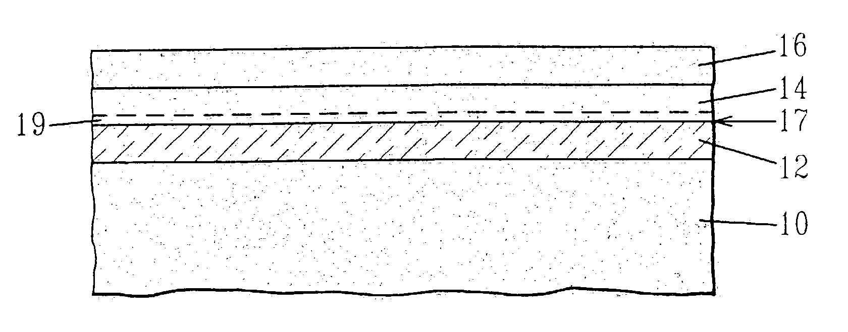
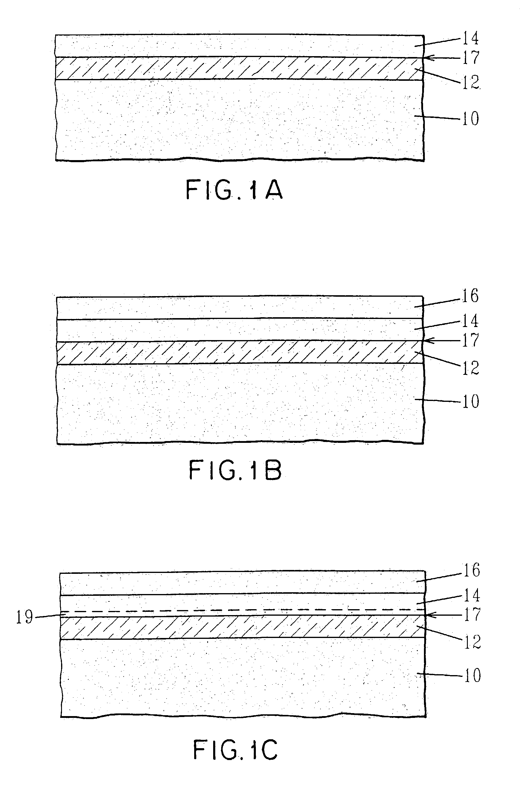
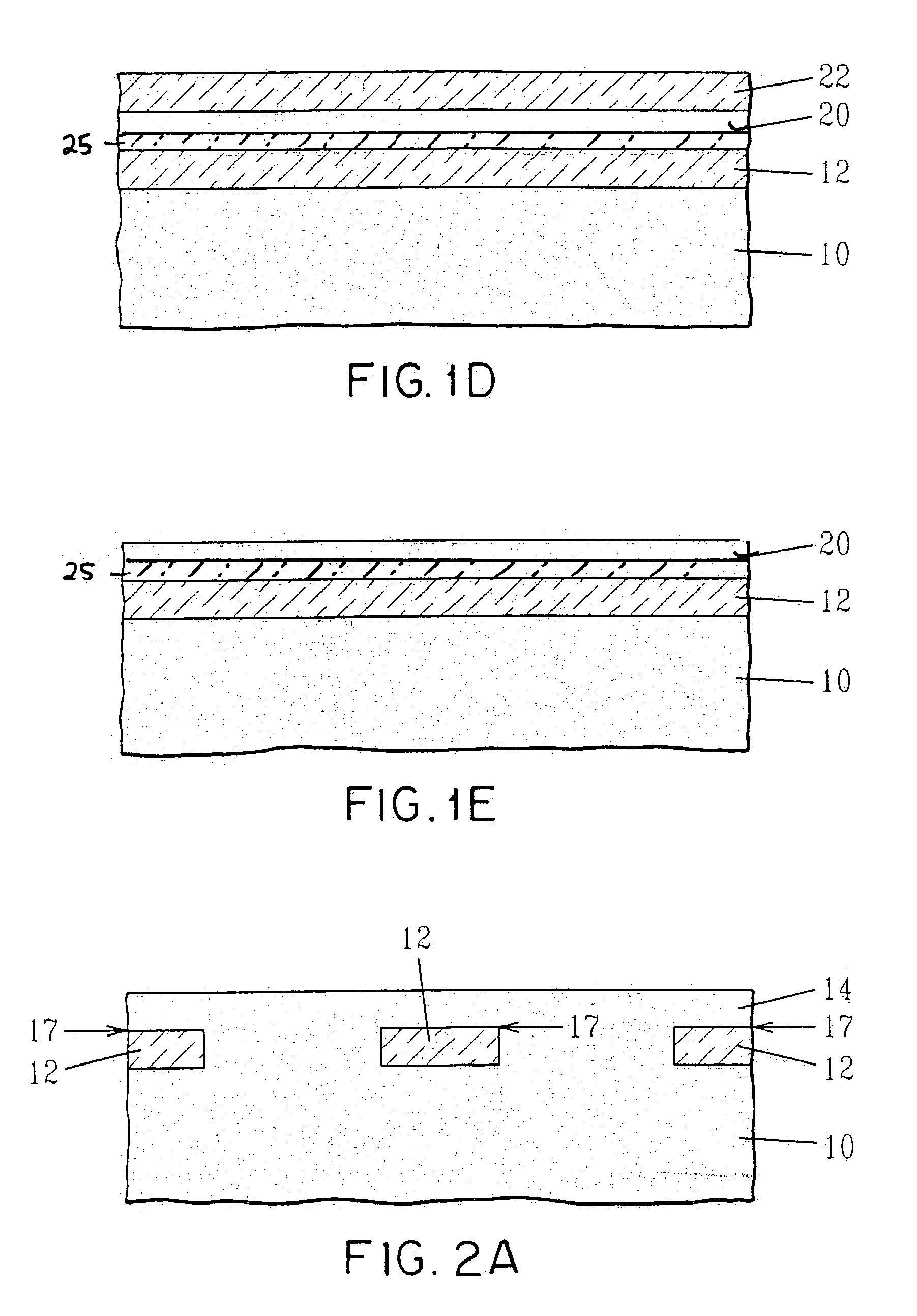
[0027] The present invention, which provides a method of fabricating thin, high-quality, substantially relaxed SiGe-on-insulator substrate materials which can then serve as a lattice mismatched template for subsequent overgrowth of epitaxial Si, will now be described in greater detail by referring to the drawings that accompany the present application. In the accompanying drawings, like and / or corresponding elements are referred to by like reference numerals.

[0028] The present application provides a method for creating a high-quality, substantially relaxed SiGe-on-insulator substrate material by consumption of a sacrificial layer that has served as a defect sink. In the present method, the sacrificial layer, which is the top Si layer of an SOI substrate, is thin and the Ge-containing layer is thick thereby relaxation of the SiGe layer takes place by plastic deformation of the underlying, thin sacrificial layer. The thin sacrificial layer gets consumed in a unique way. Oxidation of ...


PUM

PropertyMeasurementUnit
temperatureaaaaaaaaaa
thicknessaaaaaaaaaa
thicknessaaaaaaaaaa

Abstract

A method of fabricating high-quality, substantially relaxed SiGe-on-insulator substrate materials which may be used as a template for strained Si is described. A silicon-on-insulator substrate with a very thin top Si layer is used as a template for compressively strained SiGe growth. Upon relaxation of the SiGe layer at a sufficient temperature, the nature of the dislocation motion is such that the strain-relieving defects move downward into the thin Si layer when the buried oxide behaves semi-viscously. The thin Si layer is consumed by oxidation of the buried oxide / thin Si interface. This can be accomplished by using internal oxidation at high temperatures. In this way the role of the original thin Si layer is to act as a sacrificial defect sink during relaxation of the SiGe alloy that can later be consumed using internal oxidation.

Description

RELATED APPLICATIONS [0001] This application is related to co-pending and co-assigned U.S. patent application Ser. No. 10 / 055,138, filed Jan. 23, 2002, entitled “Method of Creating High-Quality Relaxed SiGe-On-Insulator for Strained Si CMOS Applications”, as well as co-pending and co-assigned U.S. patent application Ser. No. 10 / 196,611, filed Jul. 16, 2002, entitled “Use Of Hydrogen Implantation To Improve Material Properties Of Silicon-Germanium-On-Insulator Material Made By Thermal Diffusion”, the entire contents of each of which are incorporated herein by reference.FIELD OF THE INVENTION [0002] The present invention relates to a method of fabricating a semiconductor substrate material, and more particularly to a method of fabricating a high-quality, substantially relaxed SiGe-on-insulator (SGOI) substrate material. The high-quality, substantially relaxed SiGe-on-insulator substrate material of the present invention can be used as a lattice mismatched template for creating a strai...

Claims


Application Information

Patent Timeline
Patent Type & Authority Applications(United States)
IPC IPC(8): H01L21/02H01L21/20H01L21/762H01L27/12
CPCH01L21/7624Y10T428/12674Y10S438/933H01L21/20
Inventor BEDELL, STEPHEN W.CHEN, HUAJIEDOMENICUCCI, ANTHONY G.FOGEL, KEITH E.SADANA, DEVENDRA K.
Owner GLOBALFOUNDRIES INC
Why Eureka
Try Eureka