Micro lead frame package and method to manufacture the micro lead frame package

a lead frame and micro-lead technology, applied in the direction of semiconductor devices, semiconductor/solid-state device details, electrical apparatus, etc., can solve the problem that the temporary connection bar does not provide an electrical connection, and achieve the effect of saving customer board spa

Active Publication Date: 2005-01-06
BEL POWER SOLUTIONS INC
View PDF14 Cites 14 Cited by
  • Summary
  • Abstract
  • Description
  • Claims
  • Application Information

AI Technical Summary

Benefits of technology

[0006] An aspect of the present invention is to provide a lead frame package that is relatively low in cost, has a relatively simple construction, and integrates a power semiconductor die and passive components within the package. In one embodiment, a micro lead frame substrate (“MLF substrate”) that includes a semiconductor die pad electrically coupled to multiple termination pads is mounted on a lead frame. The semiconductor die pad is adapted to receive a power semiconductor die (e.g., a MOSFET), a controller ASIC, a PWM controller, or the like. The termination pads are adapted to receive discrete passive components (e.g., resistors and capacitors) or a bonding wire. All of the semiconductor components are therefore located within the same package.
[0008] Yet, another aspect of the present invention is to provide a MLF substrate for a semiconductor package. In one embodiment, the lead frame includes a housing with a center pad and leads around its periphery. The MLF substrate mounts on the center pad of the lead frame and is electrically coupled to the leads. Thus, the lead frame package includes discrete passive components and saves customer board space. In another embodiment, the MLF substrate is mounted directly onto the customer board, so that heat generated by a power semiconductor die is dissipated directly into the customer board. In yet another embodiment, only the semiconductor die pads and the leads of the MLF substrate contact the customer board. The bottom surface of the MLF substrate has a stepped feature whereby the contact pads (e.g., power semiconductor die pads, controller pads, and leads) are thicker than the non-contact portions of the MLF substrate (e.g., permanent connection bars).

Problems solved by technology

The temporary connection bars do not provide an electrical connection between termination pads in the final lead frame package.

Method used


Image

  • Micro lead frame package and method to manufacture the micro lead frame package
  • Micro lead frame package and method to manufacture the micro lead frame package
  • Micro lead frame package and method to manufacture the micro lead frame package

Examples


Embodiment Construction

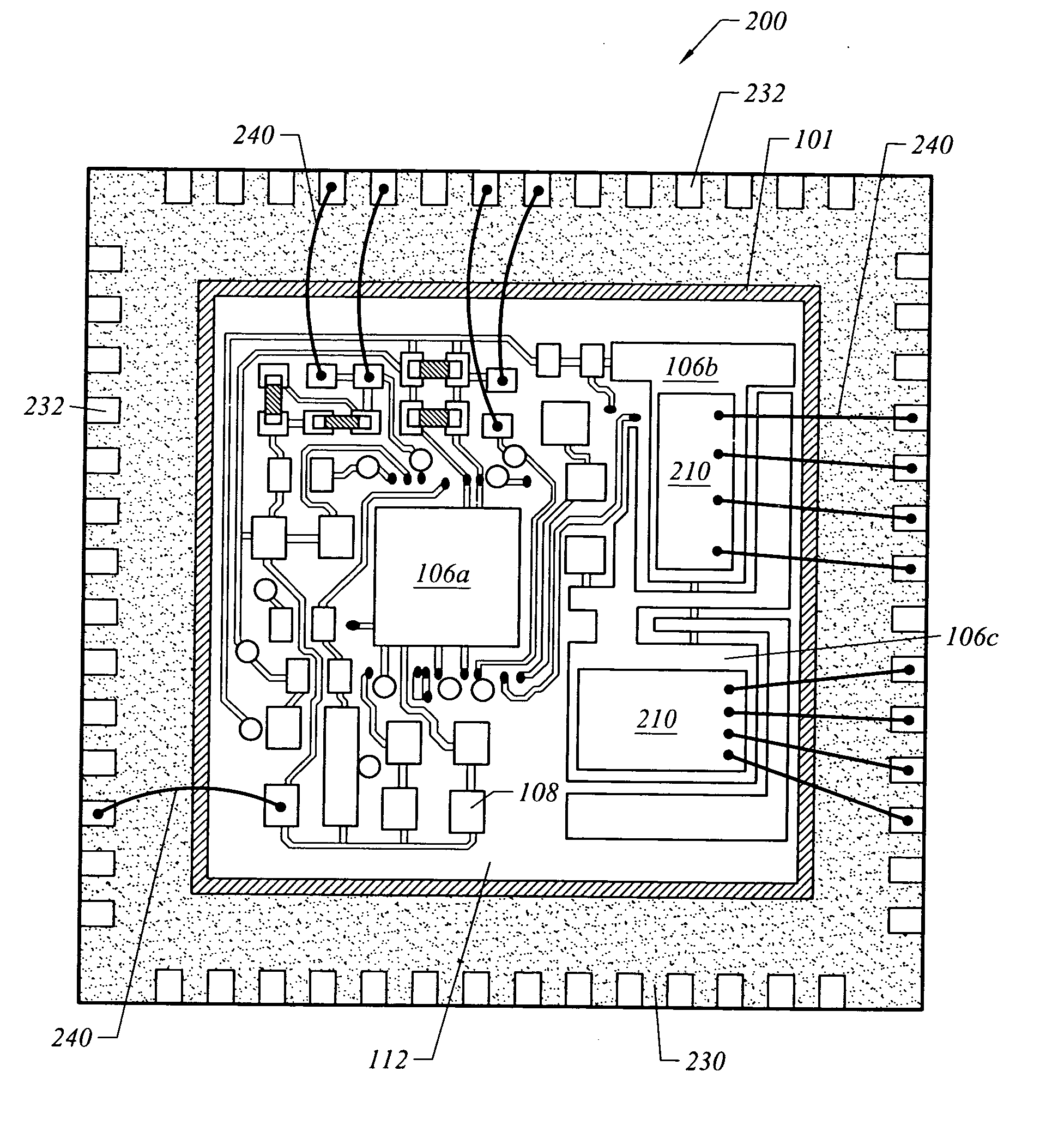
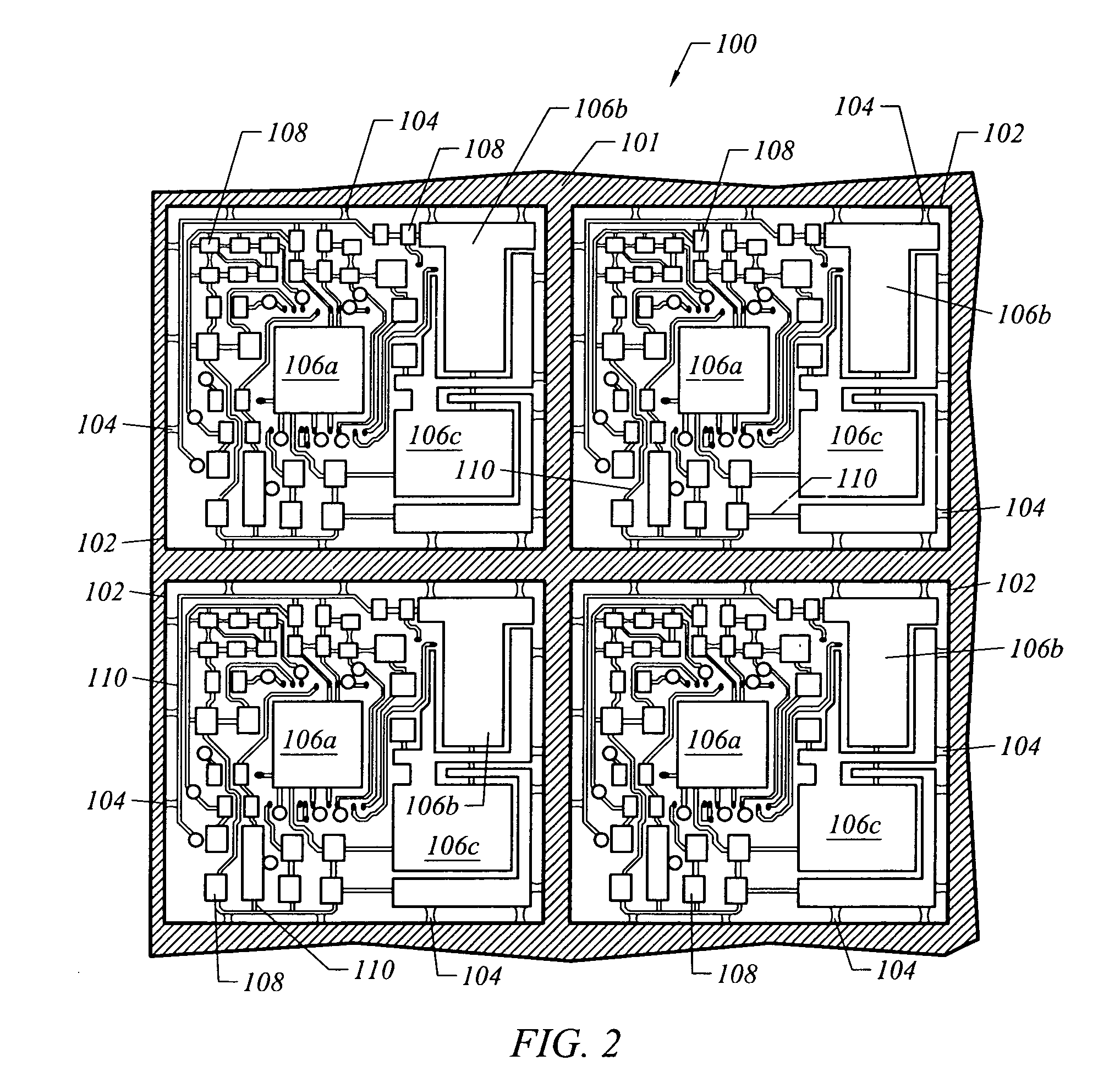
[0019] Several embodiments of the present invention will now be described with reference to FIGS. 2-9. In general, the present invention provides an MLF substrate that allows power semiconductor components, as well as passive components, to be mounted within the same package. The invention can be applied to, but is not limited to, providing optimum thermal performance within a package that requires multiple or single silicon die combined with single or multiple passive components. The invention may replace existing micro lead frame products that require external passives by placing the external components within the package, and thus reducing space and cost.

[0020]FIG. 2 illustrates a lead frame template 100 according to one embodiment of the present invention. The lead frame template 100 is preferably manufactured from a single sheet of thermally and electrically conductive material 101. Copper (Cu), a Cu-based alloy, iron-nickel (Fe—Ni), a Fe—Ni-based ally, or the like is preferab...


PUM


Abstract

The present invention comprises a lead frame substrate adapted to receive semiconductor die and multiple passive components. The lead frame substrate is preferably formed from a single piece of electrically conductive material, such as copper, and may be mounted within a lead frame package or directly onto a circuit board. The lead frame substrate includes mounting surfaces adapted to receive the semiconductor dice and passive components. The mounting surfaces are linked together by temporary and / or permanent connection bars. A method to manufacture the lead frame package includes, among other steps, forming a lead frame substrate, applying a molding compound to the lead frame substrate to fix each mounting surface and connection bar in place, removing the temporary connection bars, mounting the semiconductor components on the lead frame substrate, and applying a packaging material over the lead frame substrate to encapsulate the semiconductor components.

Description

FIELD OF THE INVENTION [0001] The present invention generally relates to the field of micro lead frame design packaging and assembly. More specifically, the present invention comprises a micro lead frame substrate that is adapted to receive at least one semiconductor die and multiple discrete passive components which may be mounted within a lead frame or directly onto a circuit board. BACKGROUND OF THE INVENTION [0002] Today's multi chip modules (MCM's) in power applications face significant challenges in terms of heat dissipation and heat management. Coupled with the need to dissipate heat in a uniform manner with low thermal impedance, there is also a need to reduce space and cost. Traditional approaches to packaging MCM's have been in the form of a Land Grid Array (LGA) or Ball Grid Array (BGA) type substrate, which consist of multiple chips (semiconductor dice) plus passive components placed on a laminate substrate. The substrate material conventionally has a high-thermal impeda...

Claims


Application Information

Patent Timeline
Patent Type & Authority Applications(United States)
IPC IPC(8): H01L21/56H01L23/31H01L23/495
CPCH01L21/561H01L21/565H01L23/3135H01L23/49575H01L24/45H01L24/49H01L24/97H01L2224/45144H01L2224/48091H01L2224/48227H01L2224/48247H01L2224/48257H01L2224/49111H01L2224/49171H01L2224/49175H01L2224/73265H01L2224/97H01L2924/01005H01L2924/01006H01L2924/01014H01L2924/01028H01L2924/01029H01L2924/01033H01L2924/01047H01L2924/0105H01L2924/01075H01L2924/01079H01L2924/01082H01L2924/13091H01L2924/14H01L2924/1433H01L2924/19041H01L2924/3011H01L24/48H01L2224/32245H01L2924/01023H01L2924/014H01L2924/10253H01L2924/1306H01L2924/00014H01L2224/85H01L2924/00H01L2924/00012H01L2924/181H01L2924/12042H01L24/73H01L23/495
Inventor KEATING, DAVID
Owner BEL POWER SOLUTIONS INC
Why Eureka
Try Eureka