Method for fabricating optical interference display cell

a technology of optical interference and display cell, which is applied in the manufacture of cable/conductor, microstructural device, crystal growth process, etc., can solve the problems of poor lateral etching capacity high cost and instability of etching xenon difluoride, and disadvantageous so as to increase the life cycle of etching plasma, reduce the time needed, increase the throughput of optical interference display

Inactive Publication Date: 2005-01-06
SNAPTRACK
View PDF2 Cites 352 Cited by
  • Summary
  • Abstract
  • Description
  • Claims
  • Application Information

AI Technical Summary

Benefits of technology

[0010] The development of the etching equipment using xenon difluoride etchant is not maturing, which is disadvantageous to the development and mass production of the optical interference display, and the etchant xenon difluoride is expensive and unstable. Therefore, if etching equipment used in semiconductor or typical planar display manufacture can be applied to perform a structure release etching process, the processing equipment of the optical interference display can be easily reorganized and consolidated, and the structure release etching process can be performed at a lower cost.

Problems solved by technology

The development of the etching equipment using xenon difluoride etchant is not maturing, which is disadvantageous to the development and mass production of the optical interference display, and the etchant xenon difluoride is expensive and unstable.
The reason that the etching equipment used in typical semiconductor or planar display manufacture is not suitable for use in the structure release etching process is the poor capacity thereof for lateral etching, and even if an etchant with a great etching property, for example, an etchant having a fluorine group or a chlorine group such as nitrogen trifluoride (NF3) or sulphur hexafluoride (SF6), is used, the etching rate is only between 3 micrometers and 10 micrometers per minute.
This is slower than that for using xenon difluoride as an etchant by several to dozens of times. Therefore, this is very disadvantageous to the throughput of the optical interference display.
Typically, since organic materials cannot resist high temperatures, the subsequent processing temperature for a construct comprised of elements made from organic composition provided therein must be kept within certain limits, typically under 250° C. Therefore, even though raising the temperature can increase the etching rate, there is still a limit as to how high the temperature can be raised.

Method used


Image

  • Method for fabricating optical interference display cell
  • Method for fabricating optical interference display cell
  • Method for fabricating optical interference display cell

Examples


Embodiment Construction

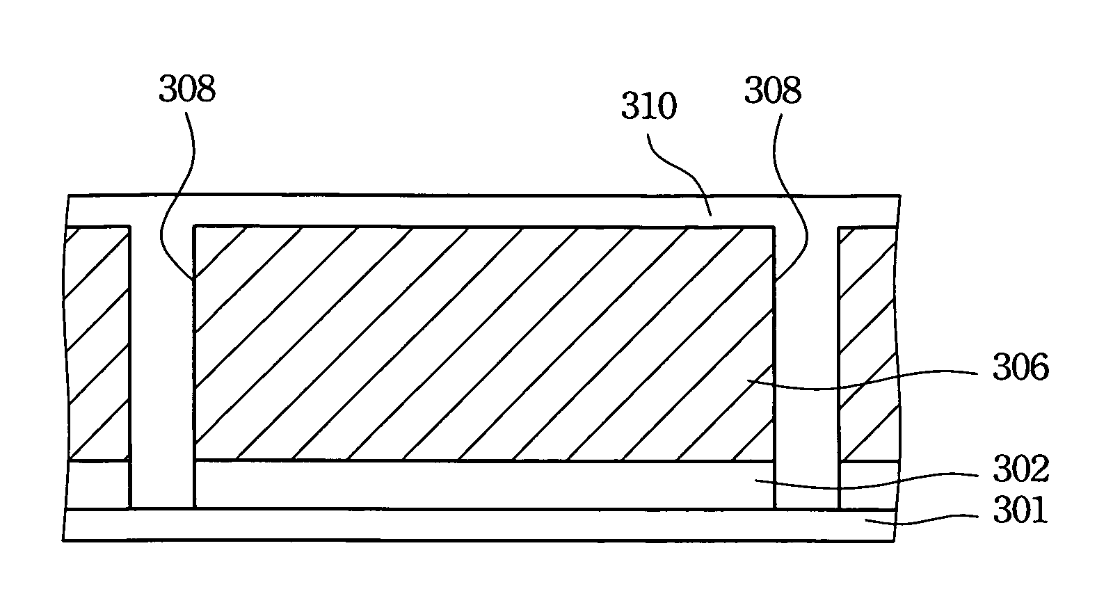
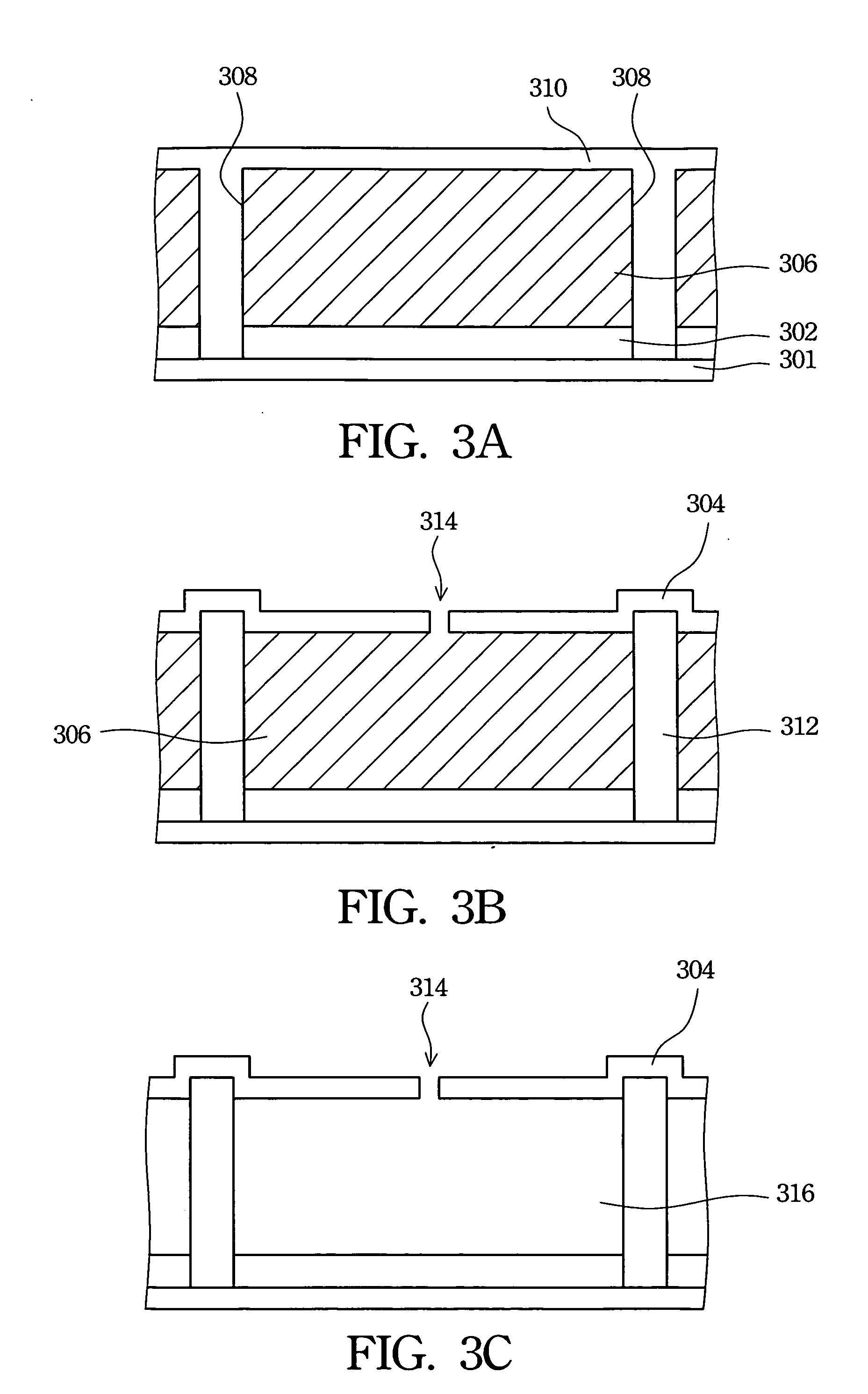
[0025] In order to make the illustration of a method for manufacturing an optical interference display cell in the present invention more clear, an embodiment of the present invention herein takes an optical interference display cell structure as an example to explain advantages of the present invention.

[0026]FIG. 3A to FIG. 3C illustrate a method for manufacturing an optical interference display cell structure in accordance with a preferred embodiment of the present invention. Referring to FIG. 3A, a first electrode 302 and a sacrificial layer 306 are formed on a transparent substrate 301 in sequence. The sacrificial layer 306 may be made of transparent material such as dielectric material, or opaque material such as metal material, polysilicon or amorphous silicon. In this embodiment, polysilicon is used as the material of the sacrificial layer 306. Openings 308 are formed in the first electrode 402 and the sacrificial layer 306 by a photolithography and etching process, and each...


PUM

PropertyMeasurementUnit
temperatureaaaaaaaaaa

Abstract

A method for fabricating an optical interference display cell is described. A first electrode and a sacrificial layer are sequentially formed on a transparent substrate and at least two openings are formed in the first electrode and the sacrificial layer to define a position of the optical interference display cell. An insulated heat-resistant inorganic supporter is formed in each of the openings. A second electrode is formed on the sacrificial layer and the supporters. Finally, a remote plasma etching process is used for removing the sacrificial layer.

Description

FIELD OF INVENTION [0001] The present invention relates to a method for manufacturing a structure of a structure release, and more particularly, the present invention relates to a structure of a structure release and a method for manufacturing the same adapted for an optical interference display cell. BACKGROUND OF THE INVENTION [0002] In a micro electro mechanical system (MEMS), the development of a sacrificial layer technique has become a key factor for manufacturing a suspended structure, such as a cantilever, a beam, a membrane, a channel, a cavity, a joint or hinge, a link, a crank, a gear or a rack, to name a few. A structure release etching process is adapted for removing a sacrificial layer, so a structure of a structure release in a micro electro mechanical system has a critical influence on the process of removing the sacrificial layer. [0003] A conventional structure release etching process is first introduced with an interference display cell as an example. The interfere...

Claims


Application Information

Patent Timeline
Patent Type & Authority Applications(United States)
IPC IPC(8): B81B7/00B81C1/00G02B26/00H01L21/302H01L21/3065H01L21/461
CPCG02B26/001B81C1/00
Inventor LIN, WEN-JIANTSAI, HSIUNG-KUANG
Owner SNAPTRACK
Why Eureka
Try Eureka