

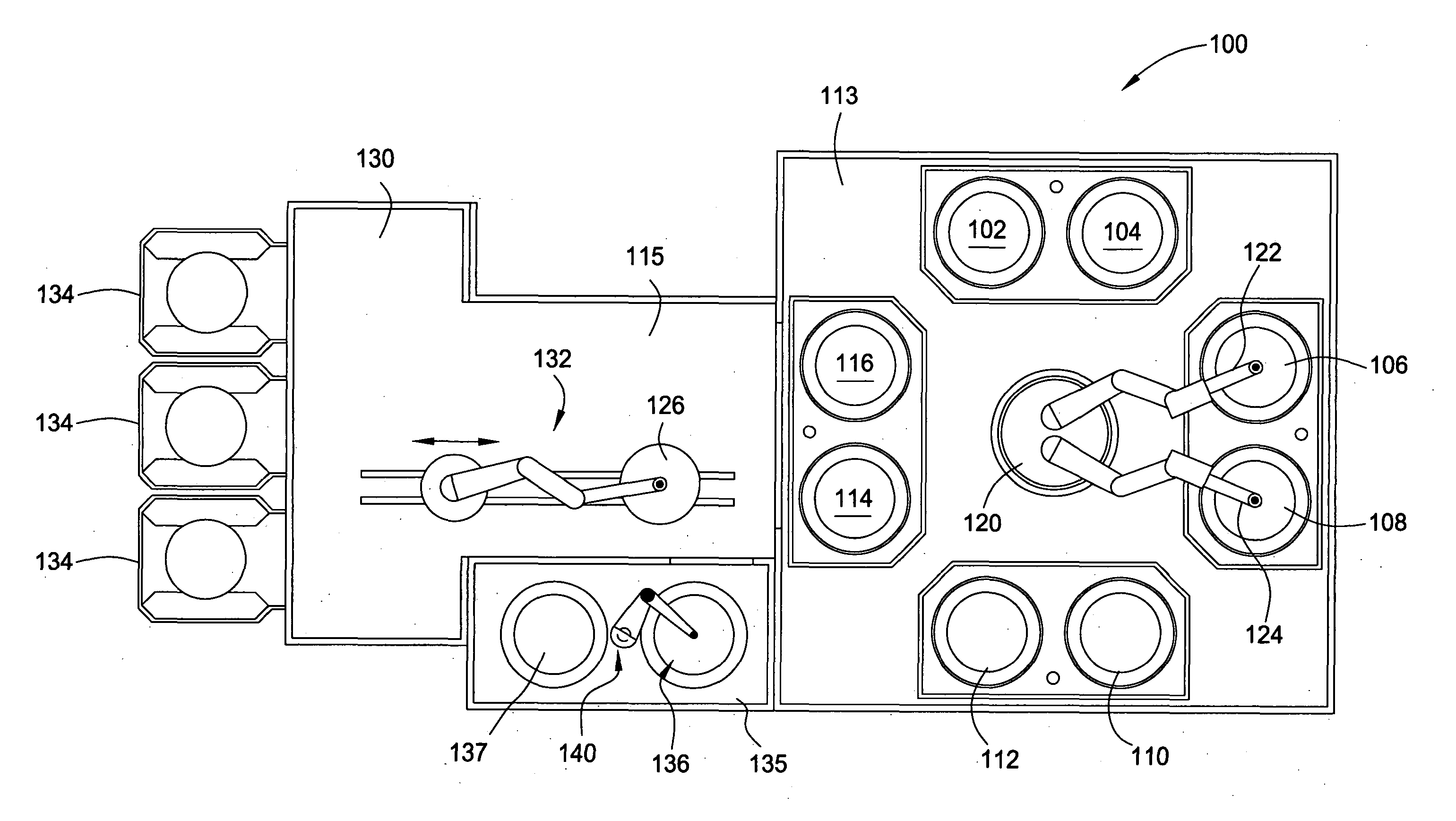
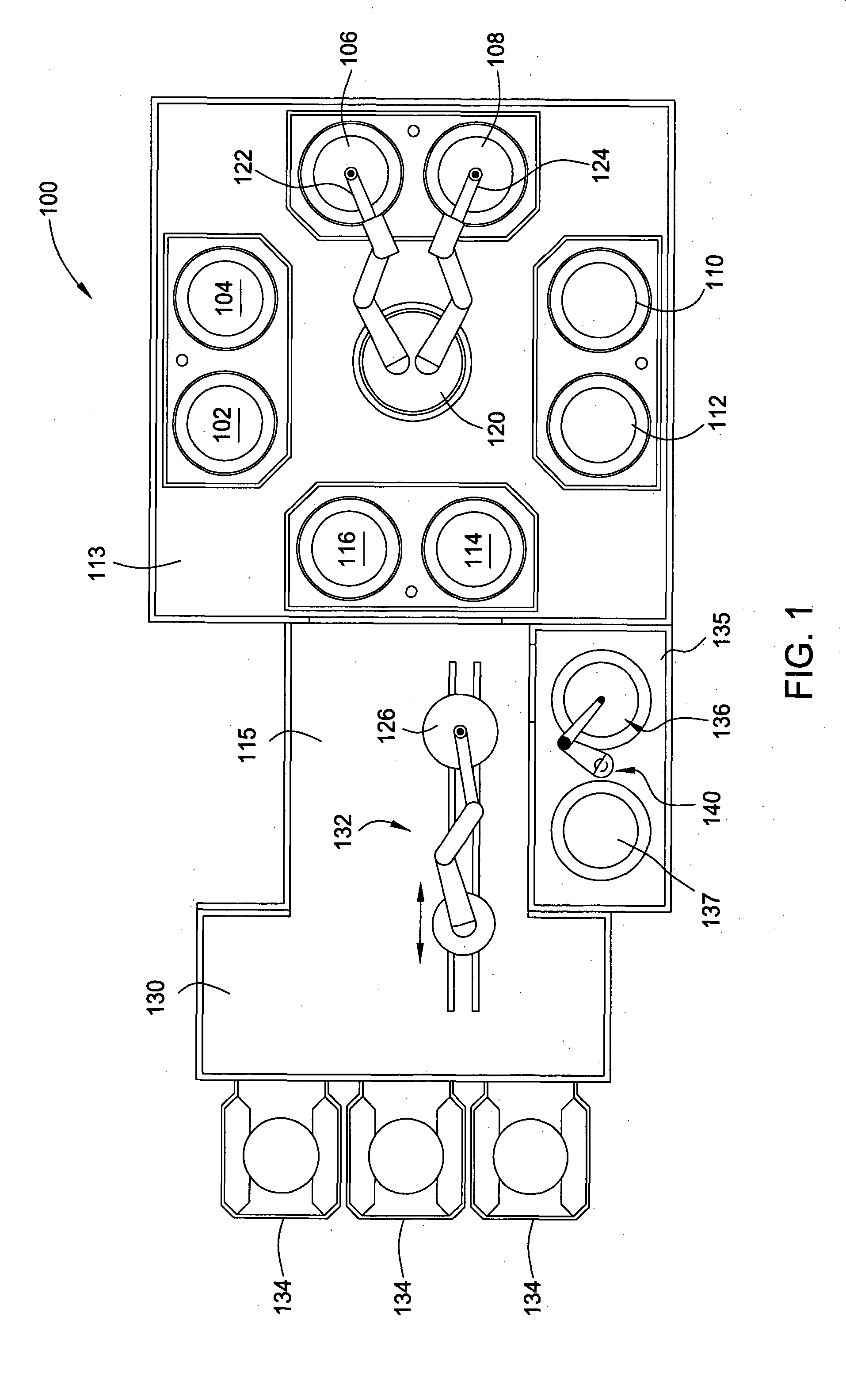
Multiple-step electrodeposition process for direct copper plating on barrier metals
a technology of barrier metals and electrodeposition processes, which is applied in the direction of basic electric elements, electrical equipment, semiconductor devices, etc., can solve the problems of insufficient support of future interconnect technology, inability to fill void-free interconnect features via conventional metallization techniques, and inability to meet the demands of future interconnect technologies
- Summary
- Abstract
- Description
- Claims
- Application Information
AI Technical Summary
Benefits of technology
Problems solved by technology
Method used
Image

Examples
example 1
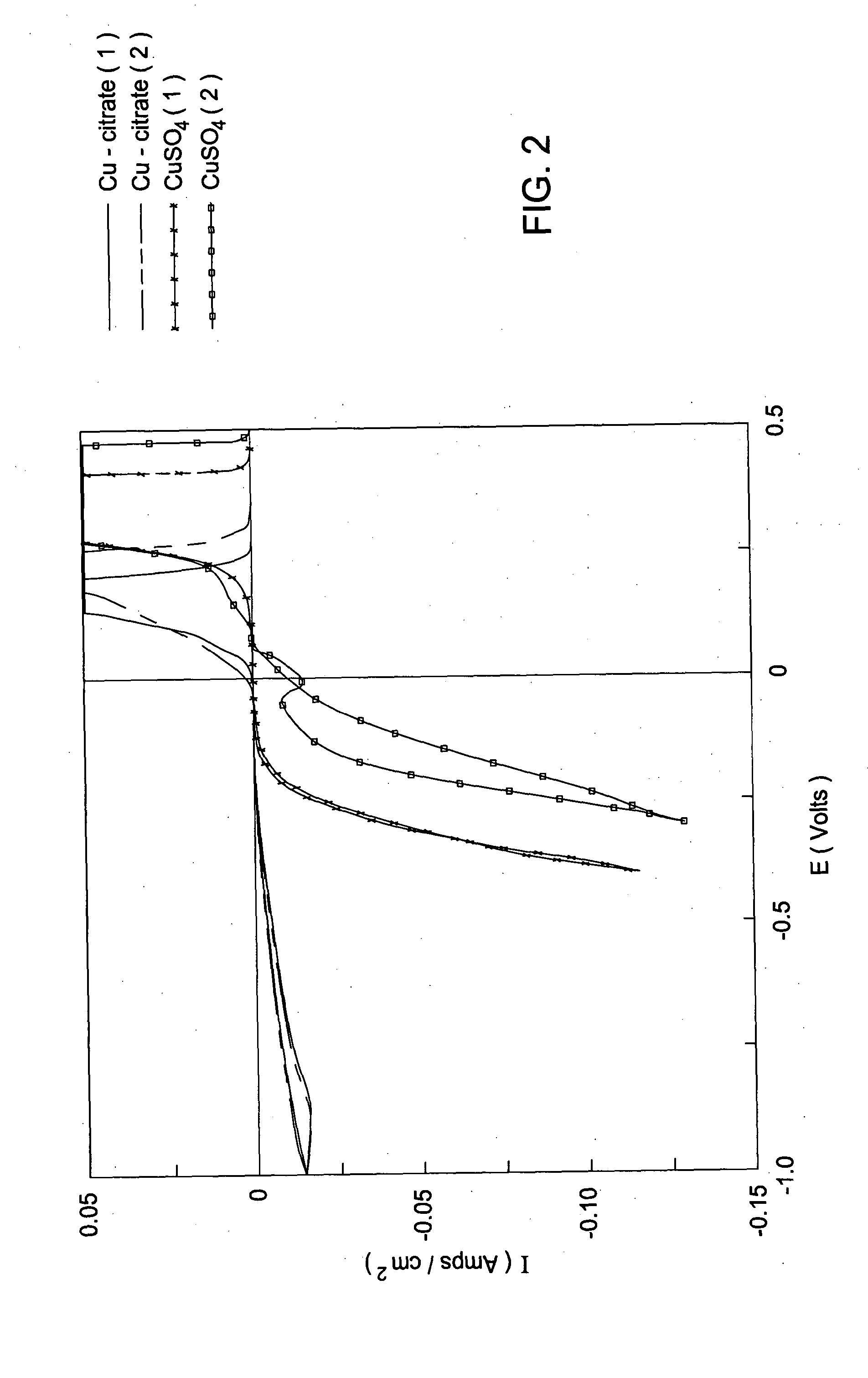
A copper seed layer was deposited onto a substrate containing a barrier layer (cobalt). The copper seed was deposited using the following plating solution within a modified cell on the Electra Cu ECP® system. A substrate was disposed in a basin containing a plating solution of: about 0.25 M copper sulfate in deionized water; and about 0.5 M sodium citrate dihydrate in deionized water.
Therefore, the plating solution had a pH of about 6. Electricity was applied at a current density of about 2 mA / cm2. The plating process continued until the seed layer was deposited to a thickness of about 100 Å.
The substrate was rinsed in deionized water for about 30 seconds while rotating at about 100 rpm and then dried via an argon gas flow. The substrate was annealed in an O2-free environment for 30 seconds, in the annealing chamber of the Electra iECP system.
After the annealing step, a gap-fill deposition step, is carried out. The gap-fill step includes a solution containing CuSO4 (0.25 M)...
example 2
A copper seed layer was deposited onto a substrate containing a barrier layer (cobalt). The copper seed was deposited using the following plating solution within a modified cell on the Electra Cu ECP® system. A substrate was disposed in a basin containing a plating solution of: about 0.25 M copper sulfate in deionized water; about 0.5 M sodium citrate dihydrate in deionized water; and about 200 ppm of polycarboxylate (EO / PO) copolymers.
The plating solution had a pH of about 5.8. Electricity was applied at a current density of about 2.0 mA / cm2. The plating process continued until the seed layer was deposited to a thickness of about 100 Å.
example 3
A copper seed layer was deposited onto a substrate containing a barrier layer (ruthenium). The copper seed was deposited using the following plating solution within a modified cell on the Electra Cu ECP® system. A substrate was disposed in a basin containing a plating solution of: about 0.3 M copper sulfate in deionized water; and about 0.5 M boric acid in deionized water.
The plating solution had a pH of about 5. Electricity was applied at a current density of about 2.0 mA / cm2. The plating process continued until the seed layer was deposited to a thickness of about 100 Å.
PUM
| Property | Measurement | Unit |
|---|---|---|
| Molar density | aaaaa | aaaaa |
| Molar density | aaaaa | aaaaa |
| Molar density | aaaaa | aaaaa |
Abstract
Description
Claims
Application Information