Semiconductor electronic devices and methods

a technology of electronic devices and semiconductors, applied in the field of semiconductor electronic devices, can solve the problems of gan devices predicted to outperform si and sic devices for power applications

Inactive Publication Date: 2005-01-13
BOARD OF RGT THE UNIV OF TEXAS SYST
View PDF4 Cites 64 Cited by
  • Summary
  • Abstract
  • Description
  • Claims
  • Application Information

AI Technical Summary

Benefits of technology

[0007] AlGaN/GaN HFETs may be candidates for future applications in high power, high-frequency, high power, and high-temperature electronics (e.g., BMD-class X-band radar systems) because of the fundamental characteristics of Group III-nitride materials. For example, in certain embodiments, a transistor having des...

Problems solved by technology

For some applications, GaN devices are predicted t...

Method used


Image

  • Semiconductor electronic devices and methods
  • Semiconductor electronic devices and methods
  • Semiconductor electronic devices and methods

Examples


example

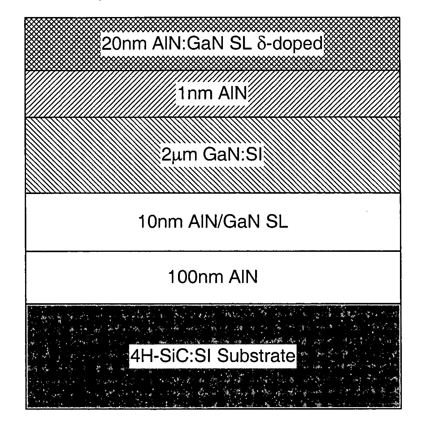
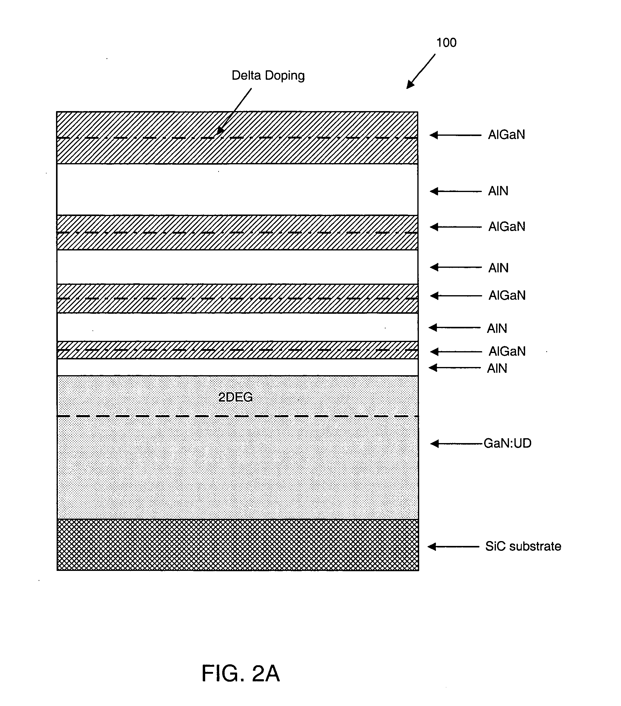
[0053] An unpassivated delta-doped, binary barrier (D2B2) HFET device with 0.15 μm-gate length was formed. The AlxGa1-xN / GaN (x≈0.2, 1.0) heterostructures of this work were grown by low-pressure metalorganic chemical vapor deposition (MOCVD) in an EMCORE TurboDisc D125 UTM high-speed rotating-disk reactor on 2.0 in. diameter 4H semi-insulating SiC substrates. The GaN epitaxial layer is grown at pressures of about 200 Torr and the AlGaN epitaxial layers are grown at about 50 Torr in a hydrogen ambient using adduct-purified trimethyl gallium (TMGa), trimethylaluminum (TMAl), and ammonia (NH3). Silane (SiH4) was used for the n-type dopant. The growth process begins with a high-temperature (about 1070° C.) AlN buffer layer, 100 nm in thickness. The subsequent device layers are grown at about 1050° C., beginning with 3 μm of undoped GaN. On top of this is a 1 nm AlN barrier layer, followed by a 30 nm layer of AlxGa1-xN (x is about 0.2). The delta doping occurs after 5 nm of growth of t...


PUM


Abstract

Embodiments disclosed herein include electronic device designs based upon electronic properties of Group III-N materials and quantum-mechanical effects of specialized heterostructures. Such electronic device designs may include, for example, heterojunction field-effect transistors (HFETs) and high-electron-mobility transistors (HEMTs). The design concepts permit high power, high-frequency, and high-temperature operation of advanced electronic circuits, including devices for radar, collision-avoidance systems, and wireless communications. Designs disclosed may include one or more AlN layers and/or one or more SMASH superlattice barriers combined with one or more n-type delta-doped regions. Alternately, in certain embodiments, one or more AlN layers and one or more SMASH superlattice barriers may be combined without the n-type delta-doped regions.

Description

PRIORITY CLAIM [0001] This application claims the benefit of U.S. Provisional Application No. 60 / 472,970 entitled “SEMICONDUCTOR ELECTRONIC DEVICES AND METHODS,” filed May 23, 2003.BACKGROUND OF THE INVENTION [0002] 1. Field of the Invention [0003] Embodiments disclosed herein generally relate to semiconductor devices. More particularly, embodiments relate to transistors having certain desired properties and methods of manufacturing such transistors. [0004] 2. Description of the Relevant Art [0005] During the past few years, there has been interest in the use of wide-bandgap semiconductors, e.g., SiC and GaN, for applications in high-power and high-temperature electronic devices (e.g., p-i-n rectifiers, heterojunction bipolar transistors (HBTs), heterojunction field-effect transistors (HFETs), and Schottky barriers). For some applications, GaN devices are predicted to out-perform Si and SiC devices for power applications. Consequently, Group III-nitride materials are receiving atten...

Claims


Application Information

Patent Timeline
IPC IPC(8): H01LH01L21/20H01L21/336H01L29/15H01L29/20H01L29/778H01L31/0328
CPCH01L21/02378H01L21/0242H01L21/02458H01L21/02507H01L21/0254H01L29/7787H01L21/02584H01L21/0262H01L29/155H01L29/2003H01L21/02576
Inventor DUPUIS, RUSSELL D.CHOWDHURY, UTTIYA
Owner BOARD OF RGT THE UNIV OF TEXAS SYST
Why Eureka
Try Eureka