Light emitting device, method of manufacturing the same and lighting equipment

Active Publication Date: 2005-01-13
NICHIA CORP
View PDF14 Cites 49 Cited by
  • Summary
  • Abstract
  • Description
  • Claims
  • Application Information

AI Technical Summary

Benefits of technology

[0021] The present inventors have made intensive studies in order to achieve the first object of the present invention and found out the following matters. That is, in a light emitting device with the heat release metallic part made of metal bonded to the packaging ceramic part by an adhesive by soldering using a brazing material as an adhesive, this brazing material cannot provide an ample buffering action against stress caused as the temperature of the metallic part and the ceramic part rises, and hence it is easy to cause a problem of warping, or break (crack) of the ceramic pa

Problems solved by technology

That is, in a light emitting device with the heat release metallic part made of metal bonded to the packaging ceramic part by an adhesive by soldering using a brazing material as an adhesive, this brazing material cannot provide an ample buffering action against stress

Method used


Image

  • Light emitting device, method of manufacturing the same and lighting equipment
  • Light emitting device, method of manufacturing the same and lighting equipment
  • Light emitting device, method of manufacturing the same and lighting equipment

Examples


example 1

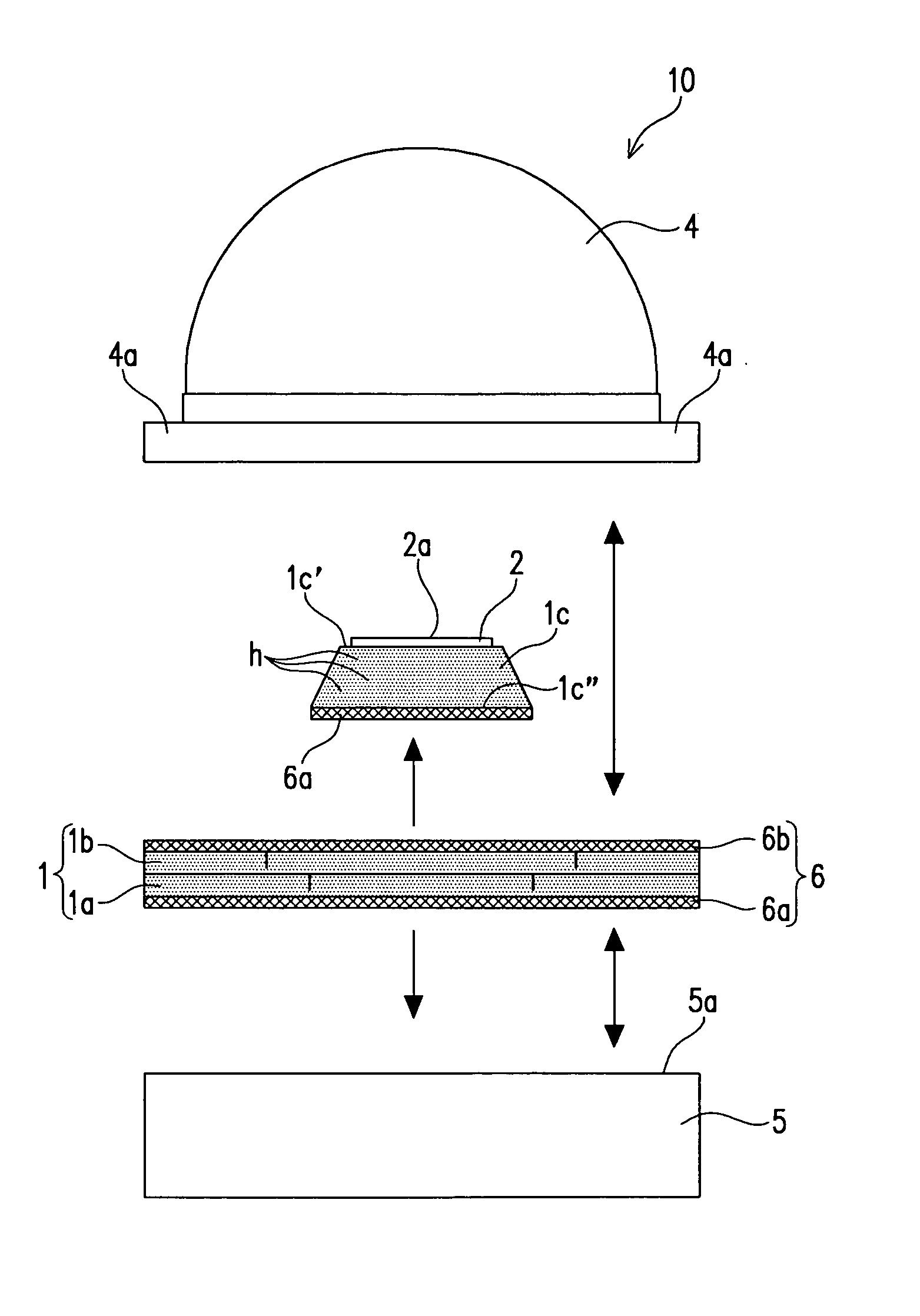
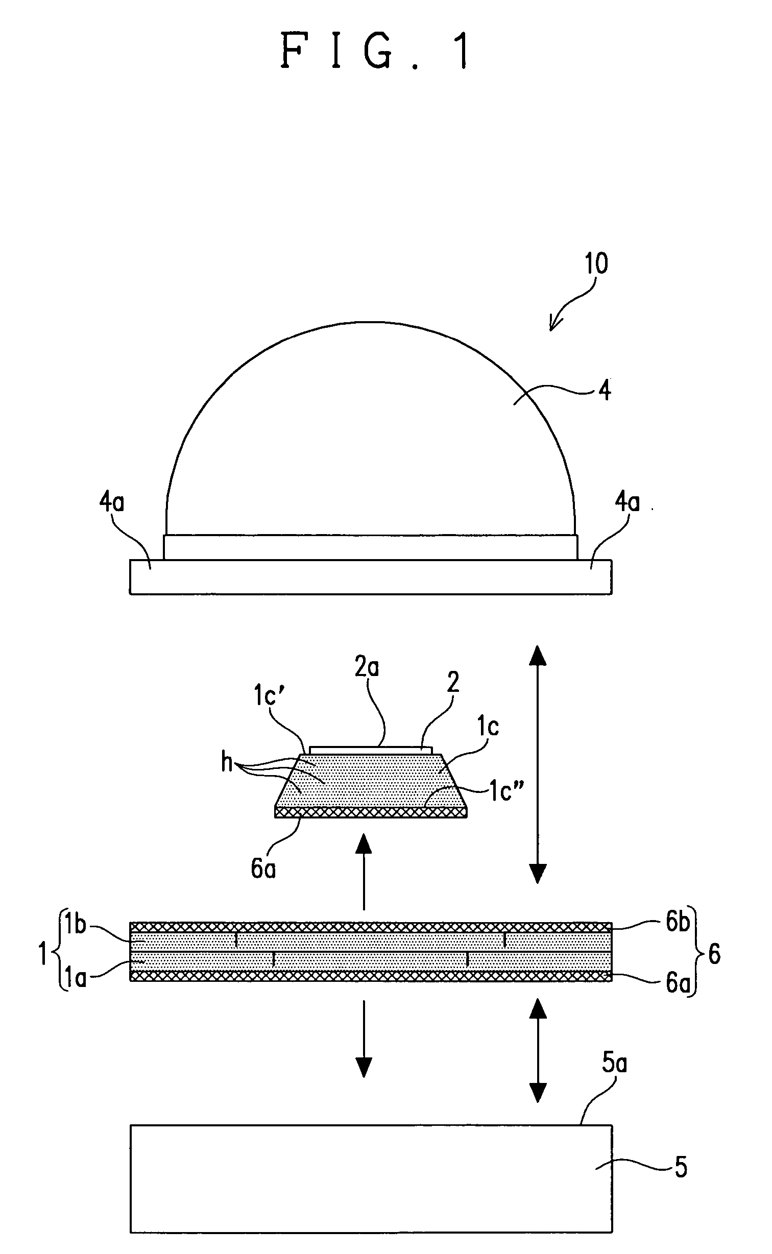
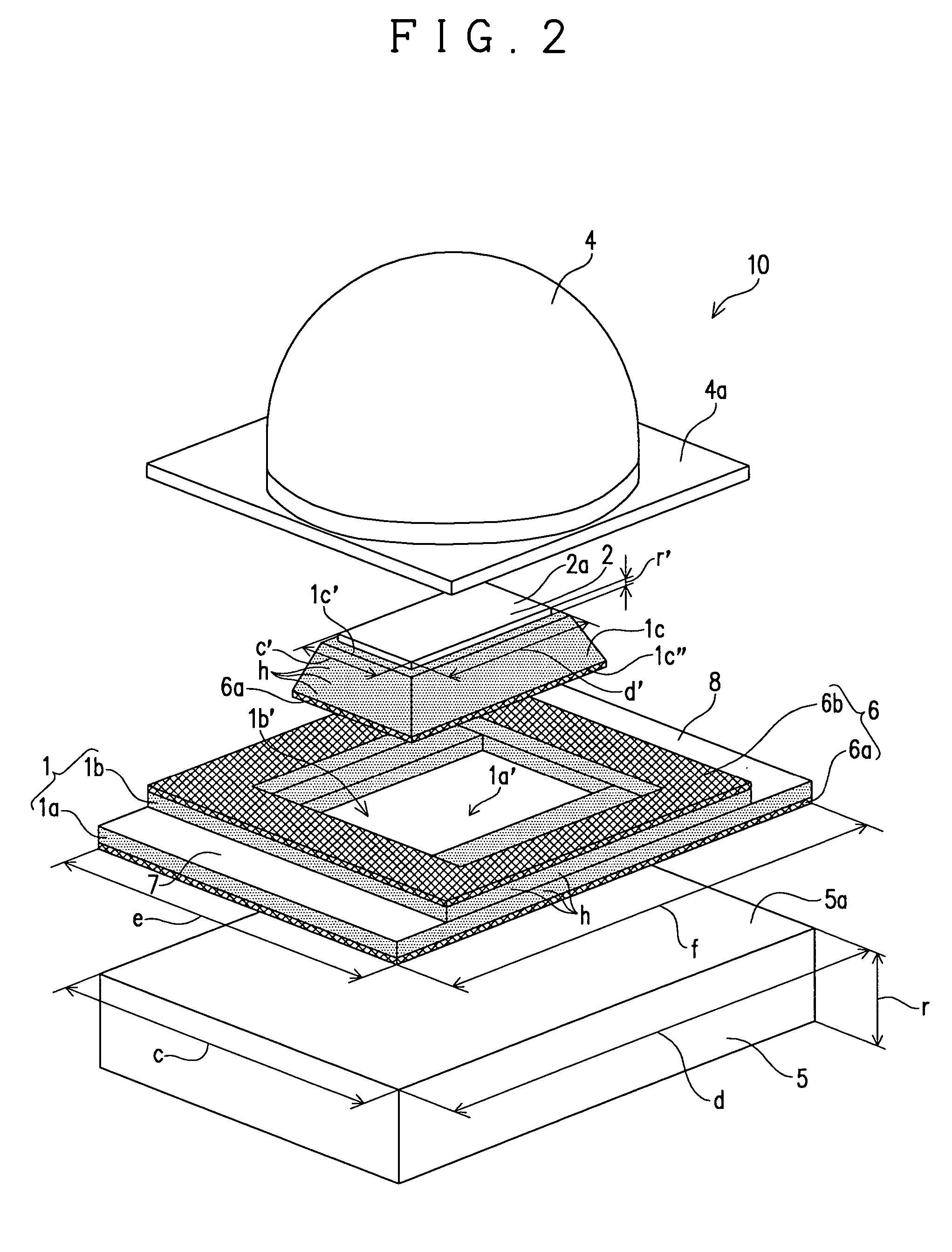
[0131] Now, the description will be made for the submount 1c of the LED 10 with reference to the relationship between the slant angle of the submount 1c of the LED 10, the temperature rise of the LED 10 and the contacting area of the bottom surface 1c″ of the submount 1c to the surface 5a of the metallic part 5 made of Cu (hereinafter referred to a Cu part), which relationship was studied by using the LED 10 of FIGS. 1-3. As illustrated in FIG. 4A, the slant angle of the submount 1c is an angle (θ in the Figure) formed by a plane R extending vertically from each side of the top surface 1c′ and a corresponding slanting surface S of the submount 1c.

[0132] Herein, the material of the ceramic part 1 is AlN and the size (e×f) is 9 mm×12 mm. The size c′×d′ of the light emitting element 2 is 1 mm×2 mm and the height r′ is 100 μm. The size of the top surface 1c′ of the submount 1c is larger than the light emitting element 2 with the width of a portion i=0.2 mm outwardly extending from the ...

example 2

[0134] Now, the description will be made for the relationship between the size c×d of the Cu part 5 (or, the package area) of the LED 10 and the difference in temperature between the light emitting element 2 and the Cu part [(temperature Tj of the light emitting element 2)−(temperature Tcu-Plate of the Cu part 5)], which relationship was studied by using the LED 10 of FIGS. 1-3.

[0135] Herein, the same conditions, elements and the like as those of the first example are applied to this example, except for the light emitting element 2, the slant angle θ of the submount 1c, and the sizes of the Cu part 5 and the ceramic part 1. As illustrated in FIG. 4B, the light emitting element 2 is comprised of eight light emitting chips arranged (in a 2×4 pattern) each having a size c″×d″=1 mm×1 mm and height r′=100 μm. The slant angle θ of the submount 1c is 20°. As the package area, the size c×d of the Cu part 5 and the size e×f of the ceramic part 1 are changed in the manner: 5 mm×5 mm (□5 mm)=...


PUM


Abstract

In a light emitting device with a heat-release metallic part made of metal and a packaging ceramic part made of ceramics bonded to the metallic part via an adhesive, the adhesive is a hot melt that melts with heat at a melting temperature higher than a given temperature and has flexibility when it has been hardened and formed a bond, and the ceramic part has pores at least in a given bonding surface region so that the hot melt is impregnated into the pores.

Description

CROSS REFERENCE TO RELATED APPLICATION [0001] This application claims priority from Japanese Patent Application Nos. 2003-272307 and 2003-357944, which are incorporated herein by reference. BACKGROUND OF THE INVENTION [0002] 1. Field of the Invention [0003] The present invention relates to a light emitting device such as a light emitting diode and a laser diode that has an excellent heat release capability, a method of manufacturing the light emitting device, and a lighting equipment using the same, in which the light emitting device is for example in the form of a light emitting diode provided with a high-electric power and high-optical power light emitting element. [0004] 2. Related Art [0005] As an typical example of the light emitting device, it can be cited an electronic device such as a light emitting diode and a laser diode. Of them, the light emitting diode (hereinafter referred to an LED) is provided with a light emitting element that is powered so as to emit light. At the ...

Claims


Application Information

Patent Timeline
IPC IPC(8): H01L33/64
CPCF21K9/00F21Y2101/02H01L33/642H01L33/486H01L33/58H01L33/641H01L2933/0033H01L2924/0002F21S48/115F21S48/215F21K9/135H01L2924/00F21K9/232F21Y2115/10F21S41/141F21S43/14
Inventor ONO, MASATO
Owner NICHIA CORP
Why Eureka
Try Eureka