Organic thin film manufacturing method and manufacturing apparatus

a technology of manufacturing method and manufacturing method, which is applied in the direction of vacuum evaporation coating, instruments, spectales/goggles, etc., can solve the problems of long time required, complex control of material heating method, and low material utilization efficiency

Inactive Publication Date: 2005-01-20
FUJI ELECTRIC HLDG CO LTD
View PDF7 Cites 47 Cited by
  • Summary
  • Abstract
  • Description
  • Claims
  • Application Information

AI Technical Summary

Benefits of technology

[0010] It is therefore an object of the present invention to provide a line source for which the various problems described above that arise during mass production are resolved, and vapor deposition over a large area is possible.

Problems solved by technology

Thus, the efficiency of utilization of the material is very low.
Furthermore, since the optimum heating conditions differ between materials that sublime and materials that evaporate after melting, there is a risk of the control of the material heating method becoming complicated.
However, the larger the evaporation source, the larger the thermal capacity, and hence a long time is required for soaking, and temperature control becomes very difficult.
For example, if a large amount of the material is consumed during mass production, then the surface of the evaporating material will drop down within the evaporation source, which may result in changes in the film thickness and the vapor deposition rate.

Method used


Image

  • Organic thin film manufacturing method and manufacturing apparatus
  • Organic thin film manufacturing method and manufacturing apparatus
  • Organic thin film manufacturing method and manufacturing apparatus

Examples


example 1

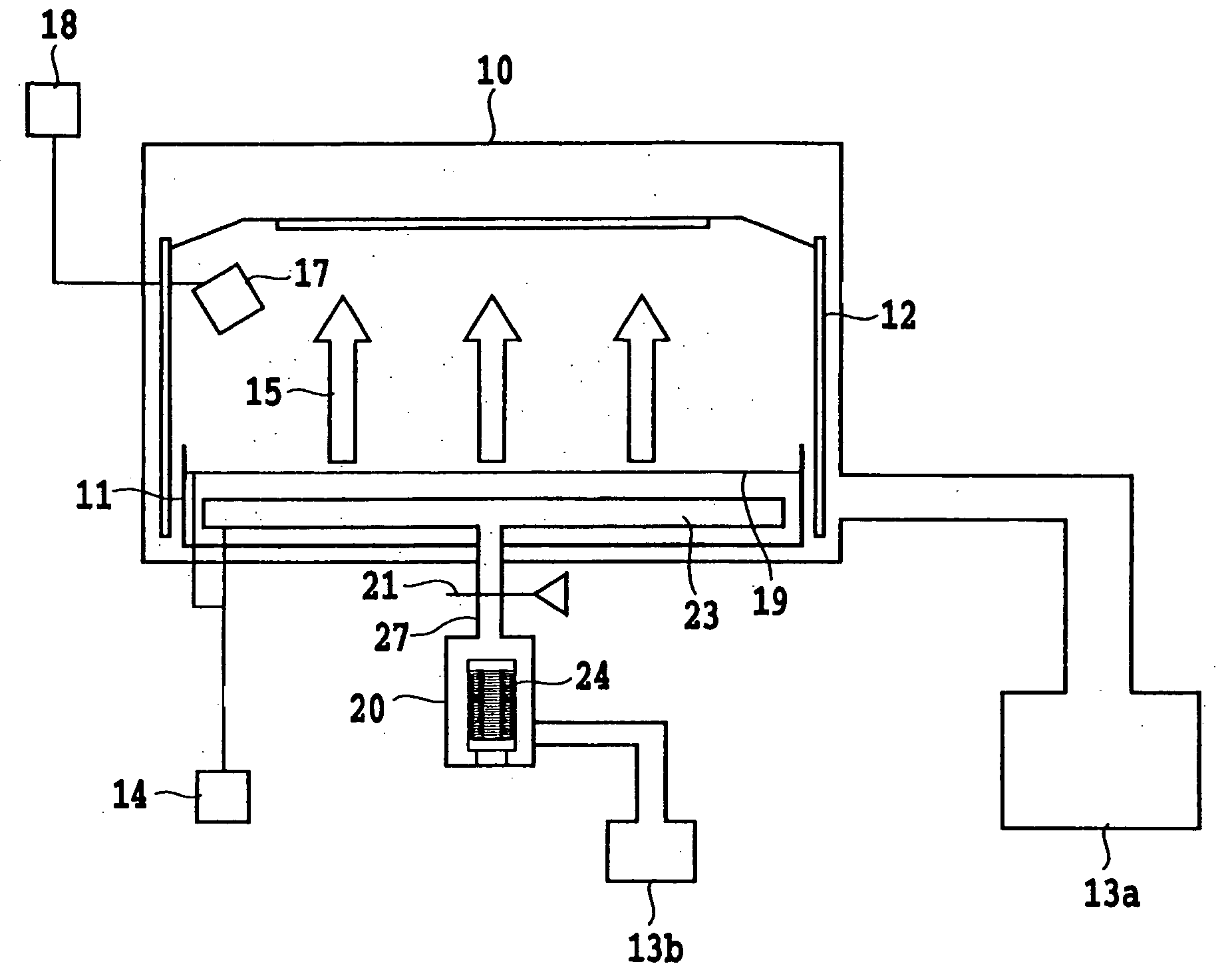
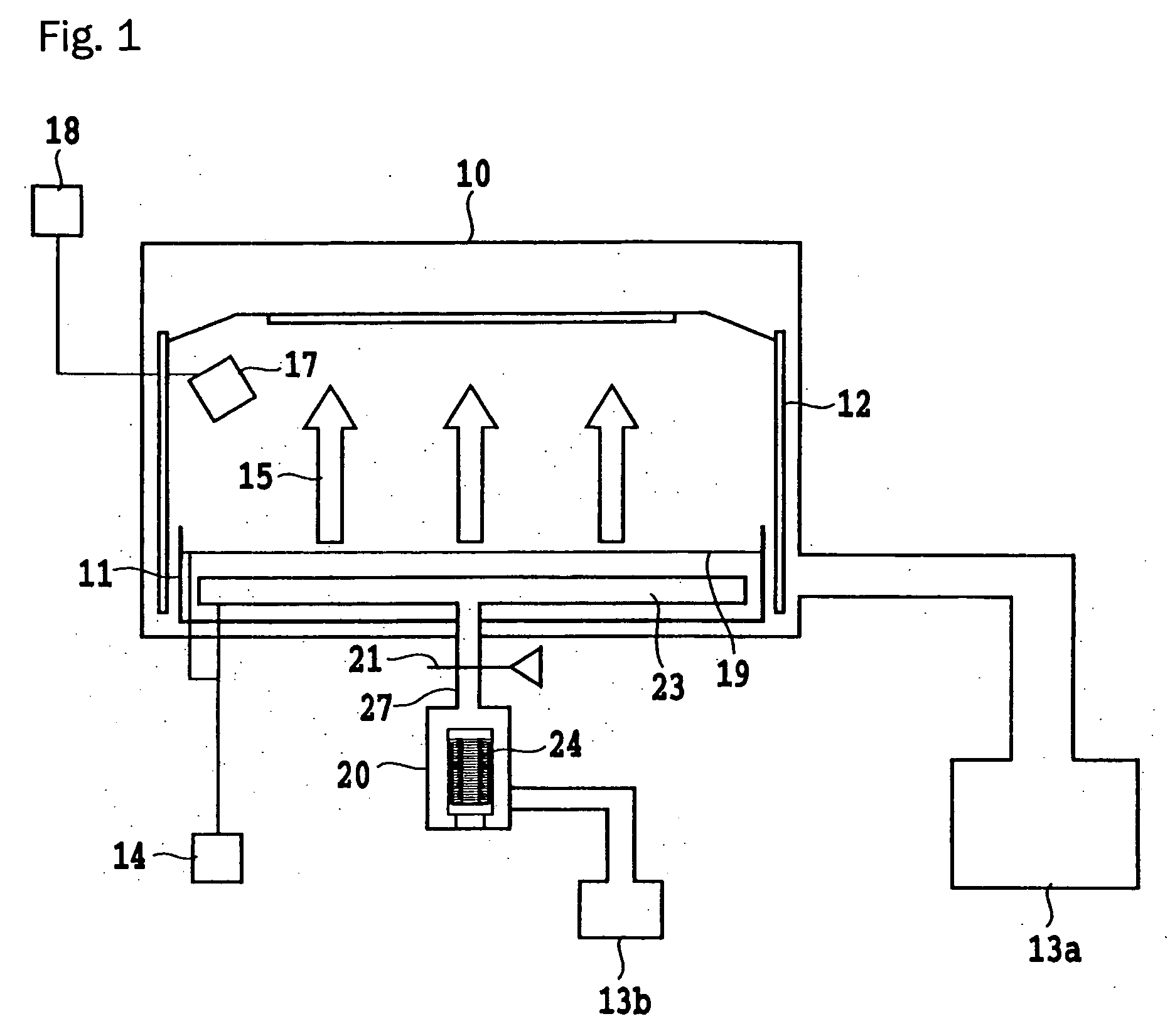
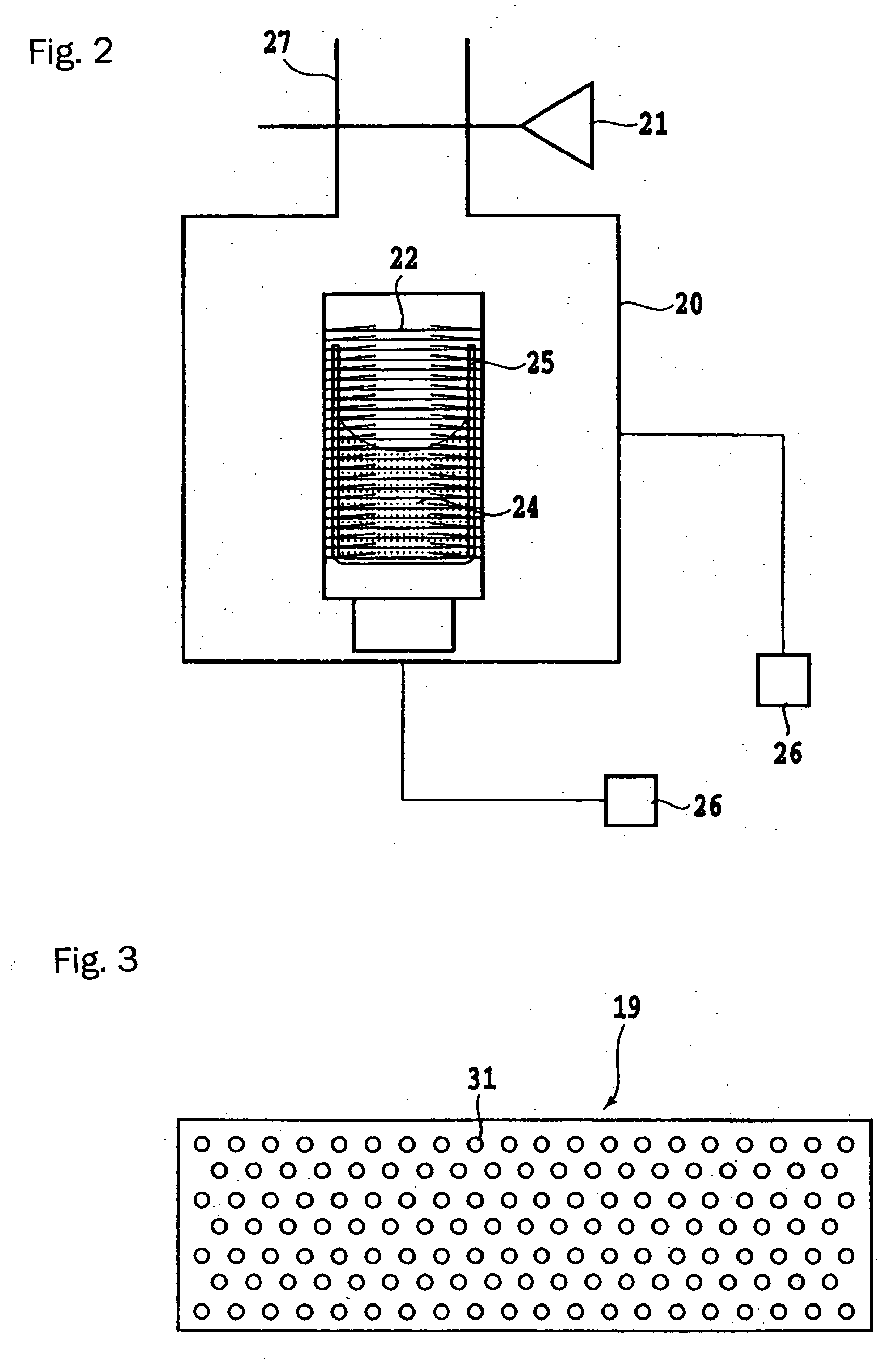
[0053] Using the film manufacturing apparatus shown in FIG. 1, a confirmatory test was carried out into the stability of the film formation rate. Glass substrates each having dimensions of 50 mm×50 mm were arranged in 15 rows by 3 columns in a substrate holder having a mounting region of dimensions 770 mm×150 mm inside vacuum chamber 10, which had an internal volume of 0.2 m3. Blocking plate 19 had dimensions of 800 mm×200 mm, and had circular stream-regulating holes of diameter 3 mm distributed uniformly over the whole thereof, with the aperture ratio (total area of stream-regulating holes / total area of blocking plate) being 0.5%. The distance between blocking plate 19 and the substrates was made to be 150 mm. Moreover, a crucible 25 having a bore diameter of 50 mm and a depth of 100 mm was provided in the material introducing part 20, which had an internal volume of 0.05 m3, and 100 g of aluminum tris-(8-quinolinolate) (Alq3) was charged into the crucible 25. Alq3 is a material th...

example 2

[0059] Using the apparatus described in Example 1, film formation was carried out over 30 seconds such that the mean film thickness would be 300 nm, thus forming Alq3 on the glass substrates.

[0060] After that, the film thickness of the organic thin film was measured for all of the glass substrates using a stylus type film thickness gauge. The result was that the film thickness variation index (the ratio of the thickness of the thinnest organic thin film to the thickness of the thickest organic thin film out of the 45 glass substrates) was 0.9 or more. This demonstrates that thin films of uniform thickness with little fluctuation in the film thickness can be formed according to the organic thin film manufacturing method of the present invention.

[0061] Furthermore, using the apparatus of the present invention, an investigation was carried out into the reproducibility of the film thickness upon carrying out film formation many times. Using the apparatus of Example 1, 30 seconds of Al...

example 3

[0065] Using the film manufacturing apparatus of Example 1, trial manufacture of organic EL devices was carried out. Three film manufacturing apparatuses according to Example 1 were linked to a vacuum vessel for conveyance having a load lock, so that substrates could be moved between the film manufacturing apparatuses without releasing the vacuum. Glass substrates (dimensions 50 mm×50 mm) on each of which an ITO film had been formed to a thickness of 100 nm were mounted, arranged in 15 rows by 3 columns, on a substrate holder having a mounting region of dimensions 770 mm×150 mm, and the substrate holder was conveyed into the vacuum vessel for conveyance from the load lock.

[0066] Next, the substrate holder was conveyed into the first film manufacturing apparatus, and an α-NPD film of thickness 40 nm was deposited at a film formation rate of 2 nm / sec, thus forming a hole transport layer on each of the substrates. The substrate holder was then conveyed into the second film manufacturi...


PUM

PropertyMeasurementUnit
pressureaaaaaaaaaa
temperatureaaaaaaaaaa
thicknessaaaaaaaaaa

Abstract

An organic thin film manufacturing method and manufacturing apparatus is disclosed in which control of the heating method of the organic material can be carried out simply, temperature control of the organic material to be subjected to vapor deposition is easy, and the reproducibility and stability of the film thickness of the organic thin film obtained are excellent. According to the organic thin film manufacturing method an organic material is fed in a vapor state into a vapor deposition apparatus positioned in a vacuum chamber from a material introducing part positioned outside the vapor deposition apparatus to form a thin film of the organic material on at least one substrate disposed inside the vapor deposition apparatus. The material introducing part has a structure such that the pressure inside can be set independently of that inside the vapor deposition apparatus, and it also has an exhauster independent to that of the vapor deposition apparatus.

Description

BACKGROUND OF THE INVENTION [0001] The present invention relates to an organic thin film manufacturing method and manufacturing apparatus. More specifically, the present invention relates to an organic thin film manufacturing method and manufacturing apparatus useful in the manufacture of organic EL devices. [0002] In recent years, there have been rapid advances in increasing the speed of, and expanding the range of application of, information communication. High-detail display devices having low power consumption and fast response that are able to answer to the requirements on display devices with regard to portability, displaying moving pictures and so on have been devised. Since the announcement by C. W. Tang of Eastman Kodak in 1987 of a high-efficiency organic EL device (hereinafter referred to as “organic EL devices”) with a two-layer laminated structure (C. W. Tang and S. A. Van Slyke, Appl. Phys. Lett., 51, 913 (1987), various organic EL devices have been developed, and some...

Claims


Application Information

Patent Timeline
Patent Type & Authority Applications(United States)
IPC IPC(8): C23C14/12C23C14/24H01L51/50H01L51/56H05B33/10
CPCC23C14/12C23C14/228H05B33/10H01L51/0008H01L51/56C23C14/243H10K71/16H10K71/00C23C14/00G02C9/04G02C5/02G02C5/12G02C7/10G02C2200/02
Inventor MATSUKAZE, NORIYUKIKIMURA, HIROSHI
Owner FUJI ELECTRIC HLDG CO LTD
Why Eureka
Try Eureka