Apparatus and method for measuring overlay by diffraction gratings

a technology of diffraction gratings and apparatus, which is applied in the direction of optical radiation measurement, instruments, spectrometry/spectrophotometry/monochromators, etc., can solve the problems of not solving the unit cells of the gratings, and achieve the effects of reducing the number of diffraction gratings, and improving the accuracy of diffraction gratings

Inactive Publication Date: 2005-01-20
TOKYO ELECTRON LTD
View PDF18 Cites 207 Cited by
  • Summary
  • Abstract
  • Description
  • Claims
  • Application Information

AI Technical Summary

Benefits of technology

An embodiment of the present invention includes an overlay target and an associated measurement instrument. The overlay target consists of multiple grating stacks, typically more than four for each of the x and y directions. Each grating stack has a different offset built into the reticle. The measurement instrument is an imaging spectrometer that captures all grating stacks in one overlay target in the field of view simultaneously. The imaging optics resolves the grating stacks but it does not resolve the unit cells of the gratings. This makes the measurement immune to lens aberrations, vibration, and focus dependency that complicates imaging-based prior art. The measurement offers ease of use and minimal preparation because it does not require computation of electromagnetic wave scattering; hence, it does not require knowledge of optic

Problems solved by technology

The imaging optics resolves the grating stacks but

Method used


Image

  • Apparatus and method for measuring overlay by diffraction gratings
  • Apparatus and method for measuring overlay by diffraction gratings
  • Apparatus and method for measuring overlay by diffraction gratings

Examples


Embodiment Construction
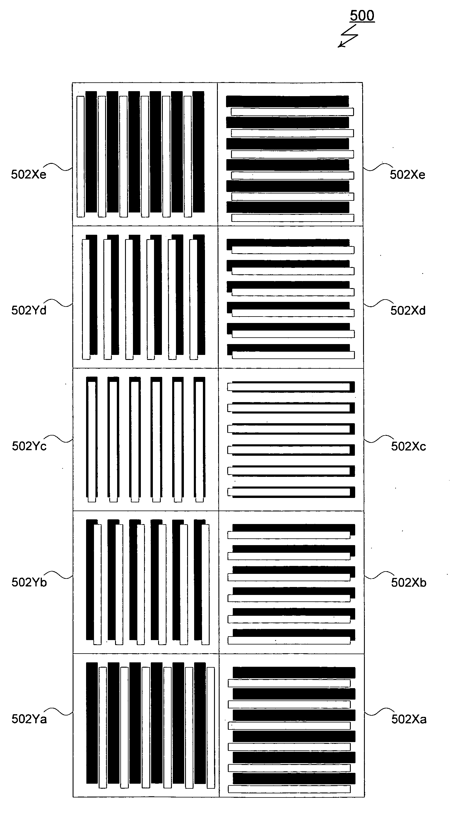
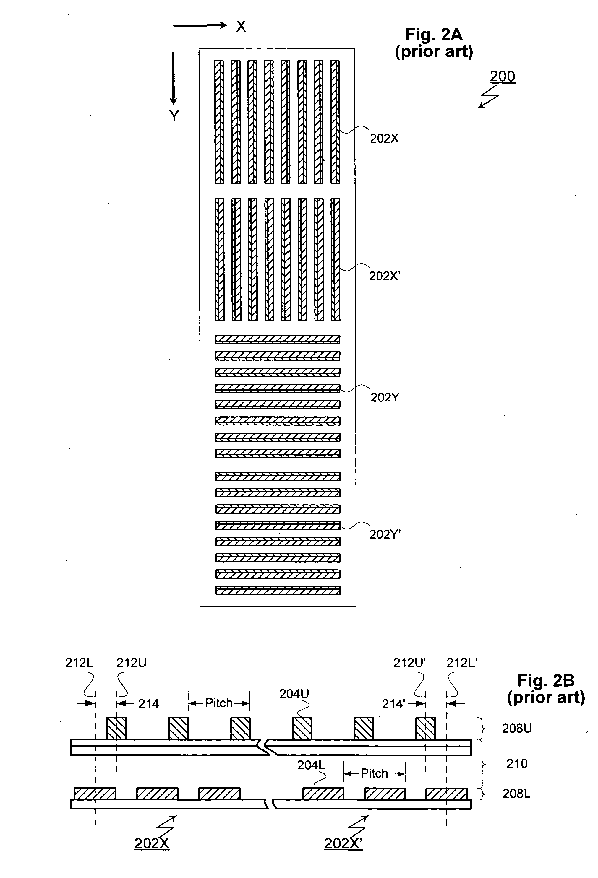
Metrology Target

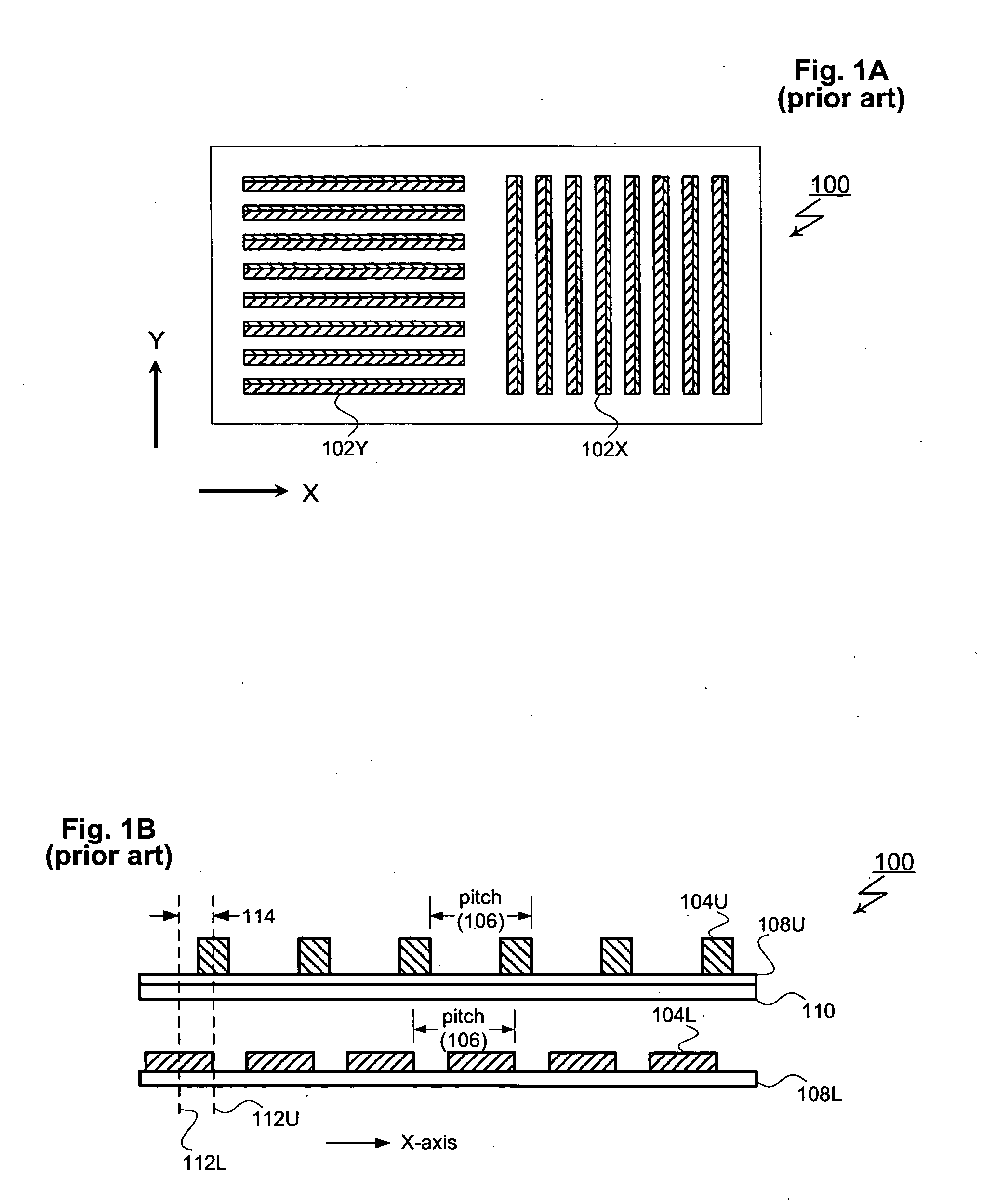
The symbol R(λ,θ,ξ) denotes the optical response of the grating stack as a function of wavelength λ, angle of incidence θ, and ξ, which denotes offset 114 in FIG. 1B. The optical response could be polarized or unpolarized reflectance or ellipsometric parameters ψ and Δ, or Fourier coefficients of intensity measured by a rotating polarizer or rotating compensator ellipsometer. Optical response R(λ,θ,ξ) has the following properties:

R(λ,θ,ξ)=R(λ,θ,ξ+Pitch)  Eq. 5a

R(λ, θ,+ε)=R(λ, θ,−ε)  Eq. 5b

R(λ, θ,(Pitch / 2)+ε)=R(λ, θ,(Pitch / 2)−ε)  Eq. 5c

Eq. 5a follows from the periodicity of the gratings. Because of reciprocity theorem of Helmholtz and symmetry of the grating lines, Eq. 5b and 5c hold for arbitrary offset ε and arbitrary angle of incidence θ. Eq. 5b follows from the symmetry of the grating stack when the centerlines of the lower and upper grating lines are aligned. Eq. 5c follows from the symmetry of the grating stack when the centerlines of the lower grating l...


PUM


Abstract

A method for measuring overlay in a sample includes obtaining an image of an overlay target that includes a series of grating stacks each having an upper and lower grating, each grating stack having a unique offset between its upper and lower grating. The image is obtained with a set of illumination and collection optics where the numerical aperture of the collection optics is larger than the numerical aperture of the illumination optics and with the numerical apertures of the illumination and collection optics are selected so that the unit cells of gratings are not resolved, the grating stacks are resolved and they appear to have a uniform color within the image of the overlay target.

Description

TECHNICAL FIELD This invention relates to measuring the alignment of a pair of patterned layers on a semiconductor wafer, possibly separated by one or more layers, made by two or more lithography steps during the manufacture of semiconductor devices. BACKGROUND OF THE INVENTION Manufacturing semiconductor devices involves depositing and patterning several layers overlaying each other. For example, gate interconnects and gates of an integrated circuit are formed at different lithography steps in the manufacturing process. The tolerance of alignment of these patterned layers is less than the width of the gate. Overlay is defined as the displacement of a patterned layer from its ideal position aligned to a layer patterned earlier on the same wafer. Overlay is a two dimensional vector (Δx, Δy) in the plane of the wafer. Overlay is a vector field, i.e., the value of the vector depends on the position on the wafer. Perfect overlay and zero overlay are used synonymously. Overlay and ove...

Claims


Application Information

Patent Timeline
IPC IPC(8): G01B11/26G01J3/28G03F7/20
CPCG01B11/26G03F7/70633G01J3/2823
Inventor SEZGINER, ABDURRAHMANSHINAGAWA, ROBERTHUANG, HSU-TING
Owner TOKYO ELECTRON LTD
Why Eureka
Try Eureka