Gas supply unit and semiconductor device manufacturing apparatus using the same

a technology of gas supply unit and semiconductor device, which is applied in the direction of coating, chemical vapor deposition coating, metallic material coating process, etc., can solve the problems of difficult process smooth progress and inability to control

Inactive Publication Date: 2005-01-27
SAMSUNG ELECTRONICS CO LTD
View PDF19 Cites 142 Cited by
  • Summary
  • Abstract
  • Description
  • Claims
  • Application Information

AI Technical Summary

Benefits of technology

[0019] Therefore, to solve the problem described hereinabove, an object of the present invention is to provide a gas supply unit capable of precisely controlling a supply flow of reaction gases supplied into the interior of a closed predetermined space such as a chamber or a furnace and a semiconductor device manufacturing apparatus using the same.

Problems solved by technology

Although the supply flow control of the reaction gases can wholly control the flow of the reaction gases supplied into the interior of the chamber, there is a drawback that the control cannot be performed when a flow control of individual reaction gases supplied into one side direction and the other side direction of the chamber is required.
However, the flow control of the entire reaction gases using the conventional MFC has a problem that a smooth progress of the process is difficult since a composition rate of the reaction gases is very important due to characteristics of the SiGe thin-film deposition process.

Method used


Image

  • Gas supply unit and semiconductor device manufacturing apparatus using the same
  • Gas supply unit and semiconductor device manufacturing apparatus using the same

Examples


Embodiment Construction

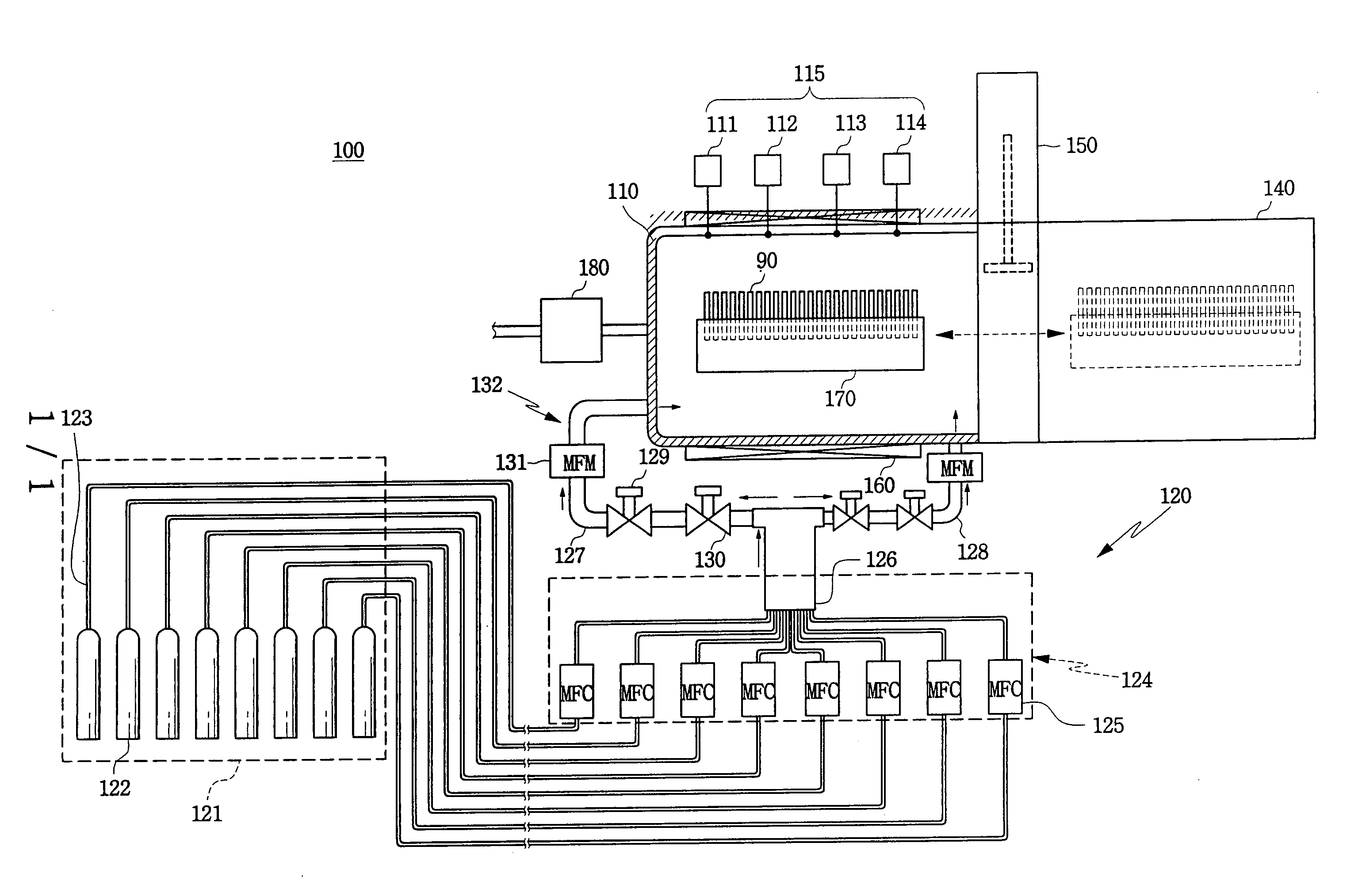
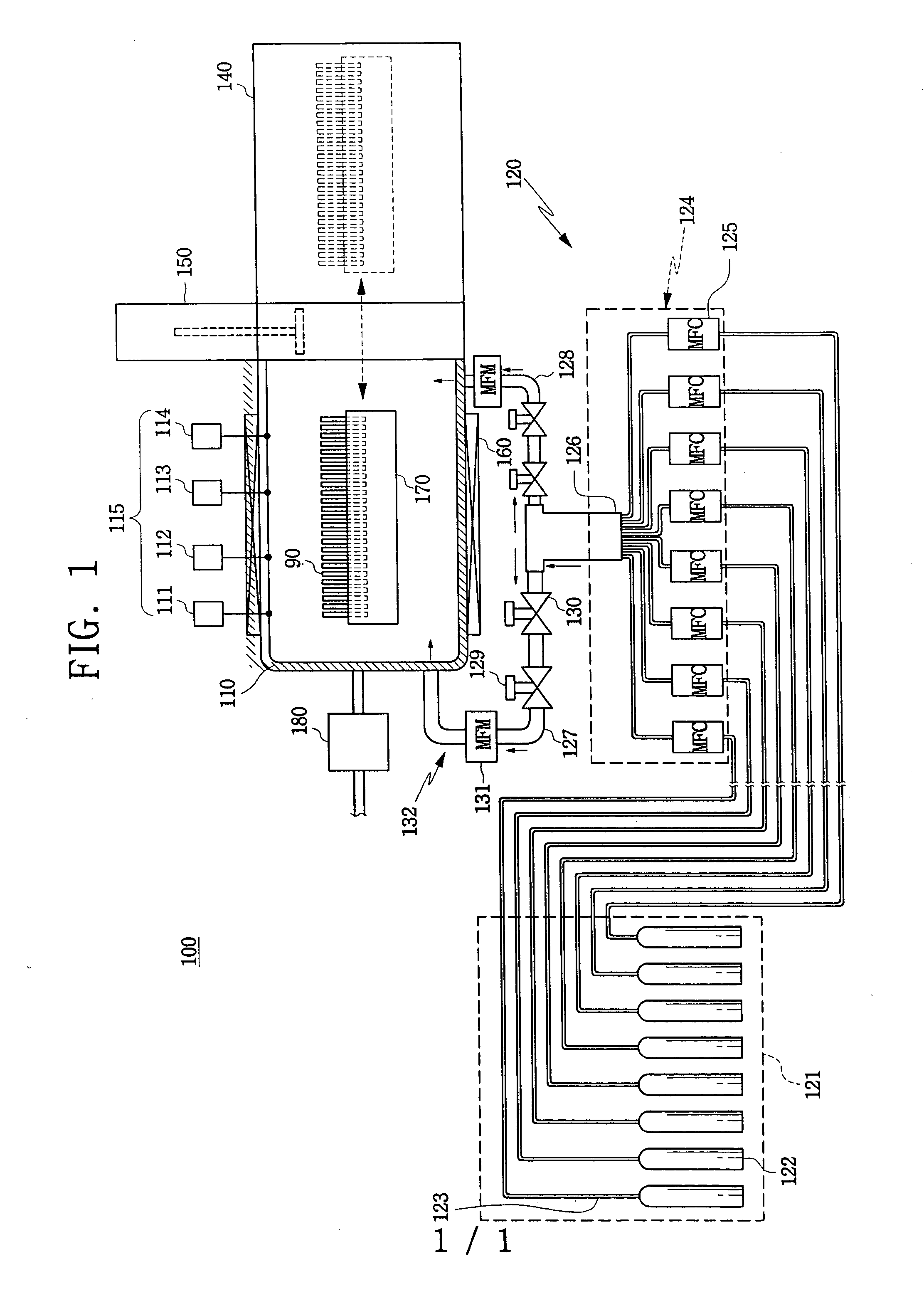
[0040] Hereinafter, the detailed description of a preferred embodiment of a gas supply unit 120 and a semiconductor device manufacturing apparatus 100 in accordance with the present invention will be apparent in connection with the accompanying drawing.

[0041] The semiconductor device manufacturing apparatus 100 in accordance with the present invention, as shown in FIG. 1, comprises a wafer boat 170 in which a number of wafers 90 are arranged sequentially. A furnace 110 has a closed predetermined space or chamber for seating the wafer boat 170 to deposit a predetermined thin-film on an upper surfaces of the wafers 90 arranged in the wafer boat 170. A loading part or member 140 is located at one side of the furnace 110 to load the wafers 90 that have undergone a prior process. A gate valve 150 is interposed between the furnace 110 and the loading part 140 to selectively open / close a pathway through which the wafer boat 170 is transferred between the furnace 110 and the loading part 1...


PUM

PropertyMeasurementUnit
pressureaaaaaaaaaa
pressureaaaaaaaaaa
pressureaaaaaaaaaa

Abstract

A semiconductor device manufacturing apparatus is provided. The semiconductor device manufacturing apparatus comprises a furnace having a closed predetermined space for seating a wafer, a loading device located at one side of the furnace to load the wafer on which a prior process may have been performed, a gate valve interposed between the furnace and the loading device to selectively open / close a pathway between the furnace and the loading device, a heater for heating an interior of the furnace, a vacuum pump for maintaining the interior of the furnace with a suitable pressure necessary to the process, a gas reservoir for storing individually various kinds of reaction gases supplied from an exterior of the space, a gas mixing device connected to the gas reservoir to mix the various kinds of reaction gases supplied from the gas reservoir with an even mixing ratio, at least two mixed gases supply pipes connected to the gas mixing device to supply the reaction gases mixed in the gas mixing device to each direction of the furnace, and a mixed gases flow control unit installed at the mixed gases supply pipe to control the flow of the reaction gases supplied through the mixed gases supply pipe.

Description

[0001] This U.S. nonprovisional patent application claims priority under 35 U.S.C. § 119 of Korean Patent Application 2003-50366 filed on Jul. 22, 2003, the entire contents of which are hereby incorporated by reference.BACKGROUND OF THE INVENTION [0002] 1. Field of the Invention [0003] The present invention relates to a semiconductor device manufacturing apparatus and, more particularly, to a semiconductor device manufacturing apparatus for depositing a predetermined thin-film on an upper surface of a wafer using a chemical vapor deposition method. [0004] 2. Description of the Related Art [0005] Generally, a semiconductor device is manufactured by repeating a process of stacking a number of thin-films into multi-layers on an upper surface of a pure silicon wafer. Therefore, a semiconductor device manufacturing process essentially includes a thin-film deposition process for depositing a predetermined thin-film on an upper surface of a wafer. [0006] The thin-film deposition process is...

Claims


Application Information

Patent Timeline
Patent Type & Authority Applications(United States)
IPC IPC(8): H01L21/205C23C16/44C23C16/455
CPCC23C16/455C23C16/45561C23C16/45557H01L21/205
Inventor RYU, SUNG-WONPARK, YEON-SIK
Owner SAMSUNG ELECTRONICS CO LTD
Why Eureka
Try Eureka