Semiconductor device

a semiconductor device and semiconductor technology, applied in the direction of electrical apparatus construction details, basic electric elements, borehole/well accessories, etc., can solve the problems of increasing ground electric noise, increasing manufacturing costs of semiconductor devices, and insufficient reduction of noise when operation becomes faster, so as to reduce noise, reduce electrical noise, and perform high-speed transmission

Inactive Publication Date: 2005-01-27
HITACHI LTD
View PDF9 Cites 24 Cited by
  • Summary
  • Abstract
  • Description
  • Claims
  • Application Information

AI Technical Summary

Benefits of technology

[0041] In this way, according to the present invention, it is possible provide a compact semiconductor device capable of reducing noise and performing high-speed transmission.
[0042] Alternatively, it is possible to provide a semiconductor device that has the minimum number of through holes compared with the number of signals to reduce electrical noise caused by high-speed operation of a large scale BGA package.

Problems solved by technology

However, with an increase in speed of operation frequency of the semiconductor device, electrical noise is increasing in ground even if the BGA package is used.
While the above known example discloses a structure to reduce ground inductance due to noise by providing multiple through holes on the ground, the noise can not be reduced sufficiently when operation becomes faster.
However, manufacturing costs for the semiconductor device will be raised.
Therefore, just the provision of multiple ground through holes results in an enlarged and complicated package, even if high-speed operation is achieved.

Method used


Image

  • Semiconductor device
  • Semiconductor device
  • Semiconductor device

Examples


embodiment 1

[0073] Embodiment 1 will be described in detail below.

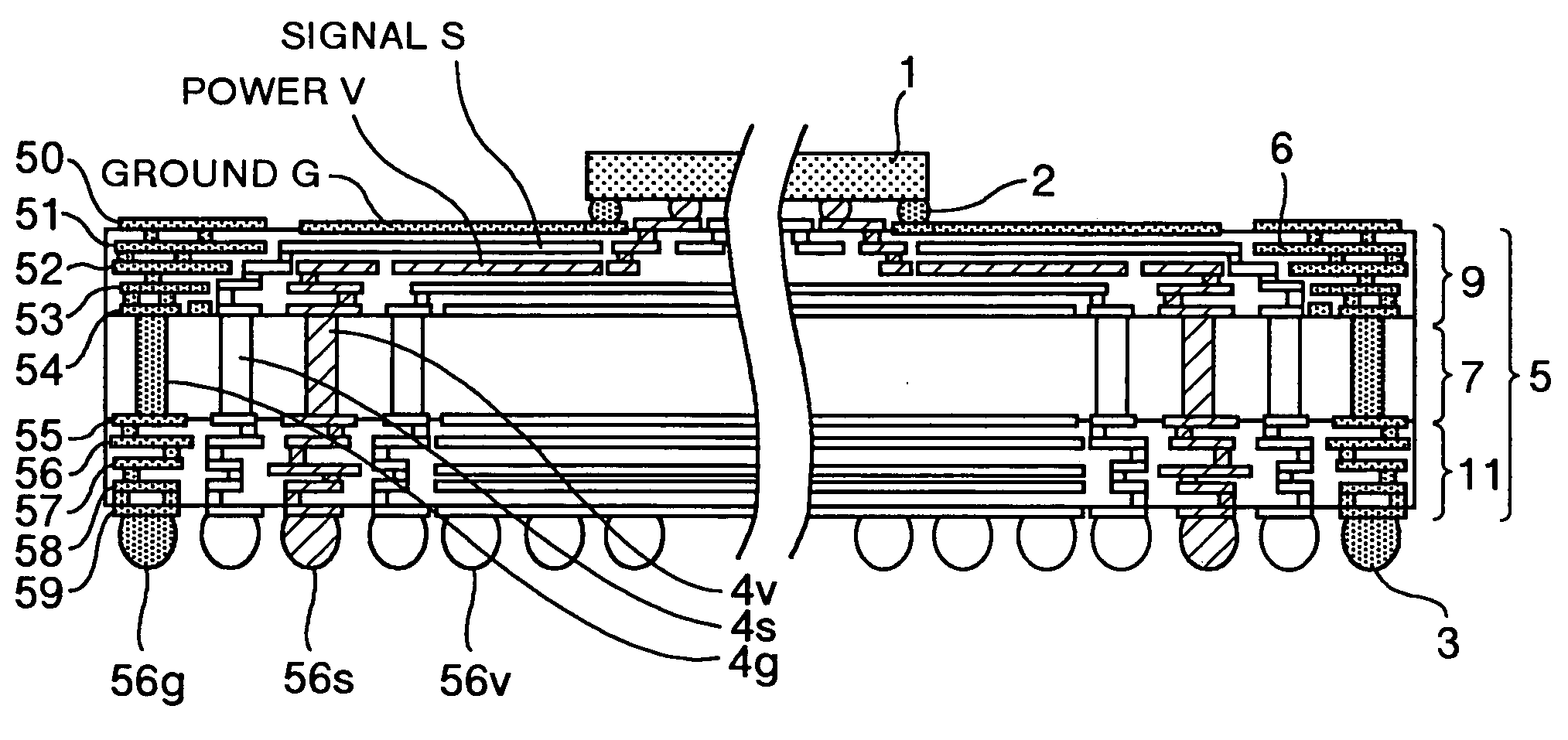
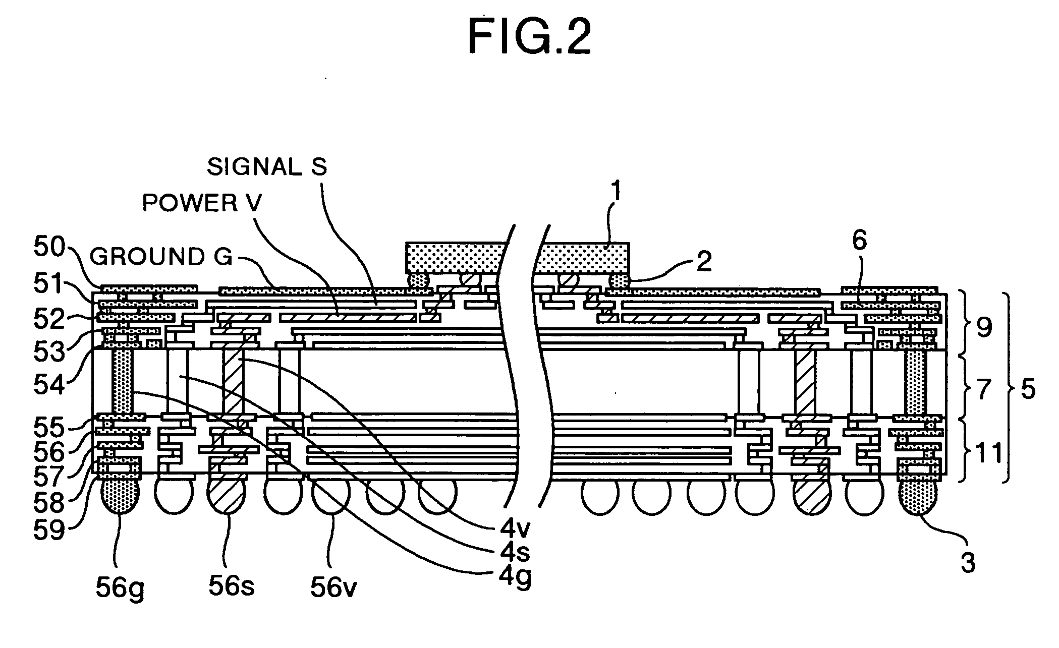
[0074]FIG. 8 illustrates a layout of through holes in the core layer 7. The through holes 4 of the core layer 7 are disposed in a grid, and inconsecutive through holes are disposed on boundaries between regions. The through hole grids are divided into an inside where potential is low and an outside where potential is high depending on the difference of potential of the power through hole. An inner through hole grid region is an inner power region 7in, while a through hole grid region outside the inner power region 7i is an outer signal region 7out. In the inner power region 7in, the through hole 4v and ground through hole 4g alternately disposed adjacent to each other. In the outer signal region 7out, through holes which do not correspond to external terminals are provided between the grids of the through holes and are connected to the conductor layers 54, and 55 which are on or under the core layer, respectively.

[0075] A trapez...

embodiment 2

[0093] Embodiment 2 will be described below.

[0094] Embodiment 2 may be identically configured with Embodiment 1. FIG. 13 shows Embodiment 2 of the BGA semiconductor device in which the layout of through holes of core layer is different. The core layer region B includes a high speed signal region 400, as shown in FIG. 13, which comprises a combination of the first signal units 300a, 300b, 301a, 301b and the second signal units 302a, 302b, 303a, 303b shown in FIG. 10. The ratio of signal through hole, power through hole, and ground through hole of the grid in the region is 6:1:1, which is due to the same reason as in the case of pattern region 300 in Embodiment 1. Inter-grid through holes may be included in the high-speed signal region. As FIG. 12 shows, transmission of signals to be transmitted among a CPU 4, an SRAM 400b, an LSI 400c, and a memory 400d, which are semiconductor devices using the BGA semiconductor devices of the present embodiment, are divided into two groups dependin...

embodiment 3

[0097] Embodiment 3 will be described below.

[0098] Embodiment 3 may basically be configured similarly to Embodiment 1. FIG. 15 shows Embodiment 3 of the BGA semiconductor in which the layout of through holes in the core layer is different. A region B of the core layer includes a high-speed bus region 500 as shown in FIG. 15 which comprises a combination of the first signal unit including 300a, 300b, 301a, 301b, and the second signal unit including 302a, 302b, 303a, 303b. The ratio of signal through hole, power through hole, and ground through hole of the grid in the region is 6:1:1, which is due to the same reason as in the case of pattern region 300 in Embodiment 1. It should be noted that inter-grid through holes may be included in the high-speed region. As FIG. 14 shows, bus 1501a, bus 2501b, and bus 3501c for transmitting a logical set of data which is dealt in one clock by LS11500a, LS12500b, LS13500c, and LS14500d, in which the BGA semiconductor of the present Embodiment 3 is ...


PUM


Abstract

A BGA semiconductor device for high-speed operation and high pin counts has a base which is constituted by a core layer formed of wiring boards and surface layers provided on both sides of the core layer, and a semiconductor element mounted on the base. Through holes in a signal region of the core layer are disposed in an optimum through hole pattern in which power through holes and ground through holes are disposed adjacent to signal through holes.

Description

BACKGROUND OF THE INVENTION [0001] The present invention relates to a semiconductor device, and more particularly, to a semiconductor device in which a semiconductor element is mounted on a base having external terminals. [0002] A BGA package has been widely used, since it is appropriate for a higher pin count package, and its inductance and noise is small because its power and ground is planar. However, with an increase in speed of operation frequency of the semiconductor device, electrical noise is increasing in ground even if the BGA package is used. [0003] As a semiconductor device for reducing the electric noise, there is a well-known example in which multiple through holes are provided in a ground pattern as disclosed in JP-A-7-153869. [0004] While the above known example discloses a structure to reduce ground inductance due to noise by providing multiple through holes on the ground, the noise can not be reduced sufficiently when operation becomes faster. [0005] The inductance...

Claims


Application Information

Patent Timeline
Patent Type & Authority Applications(United States)
IPC IPC(8): H01L23/12H01L23/498H01L23/50
CPCH01L23/49827H01L23/49838H01L23/50H01L2924/3011H01L2924/01078H01L2924/15173H01L2924/15311H01L2224/16
Inventor IIDA, TAKASHINAGATA, TATSUYAMIYAMOTO, SEIJIMATSUNAGA, TOSHIHIRO
Owner HITACHI LTD
Why Eureka
Try Eureka