FET channel having a strained lattice structure along multiple surfaces

Active Publication Date: 2005-01-27
MICROSOFT TECH LICENSING LLC
View PDF9 Cites 145 Cited by
  • Summary
  • Abstract
  • Description
  • Claims
  • Application Information

AI Technical Summary

Benefits of technology

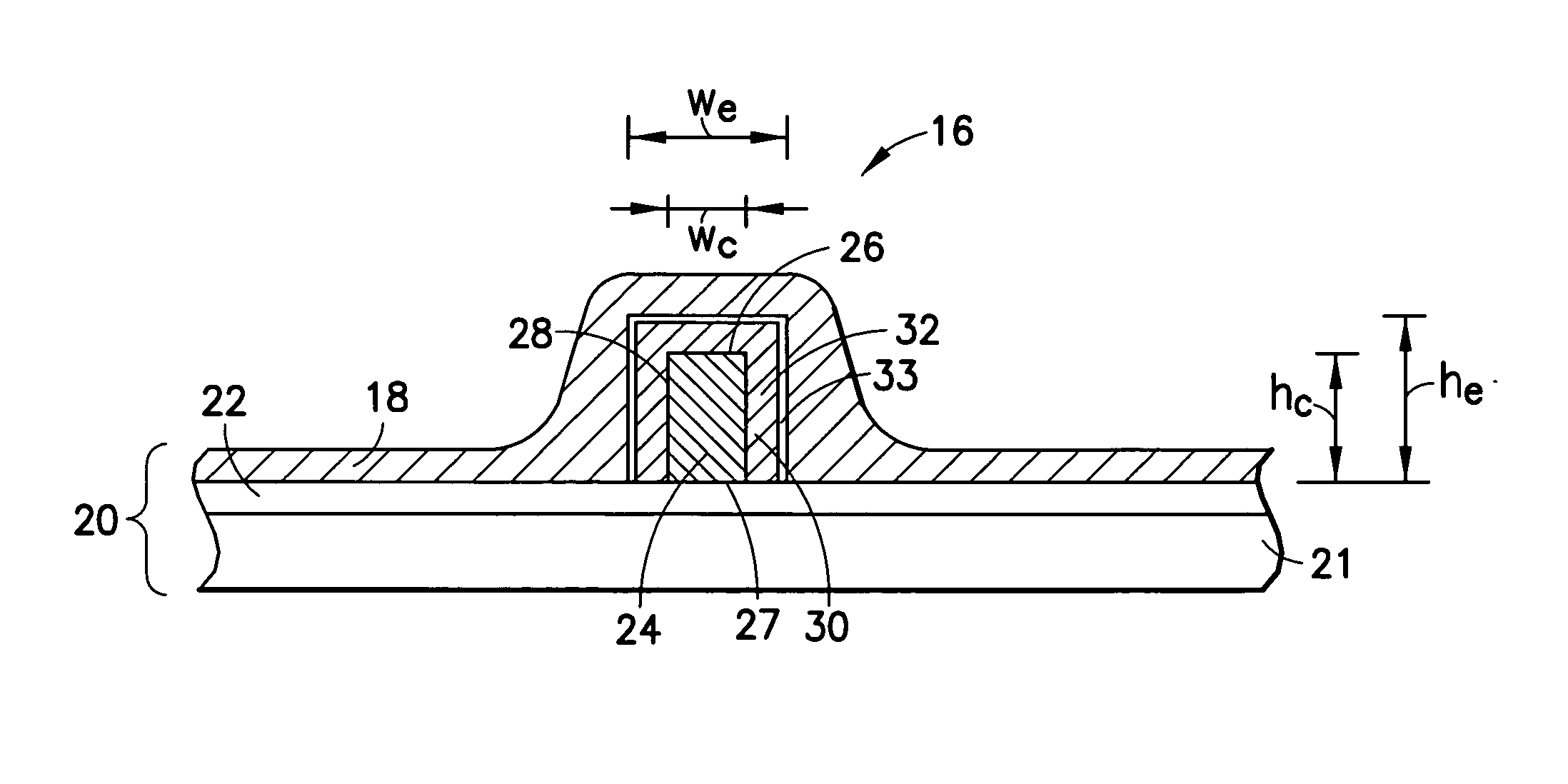
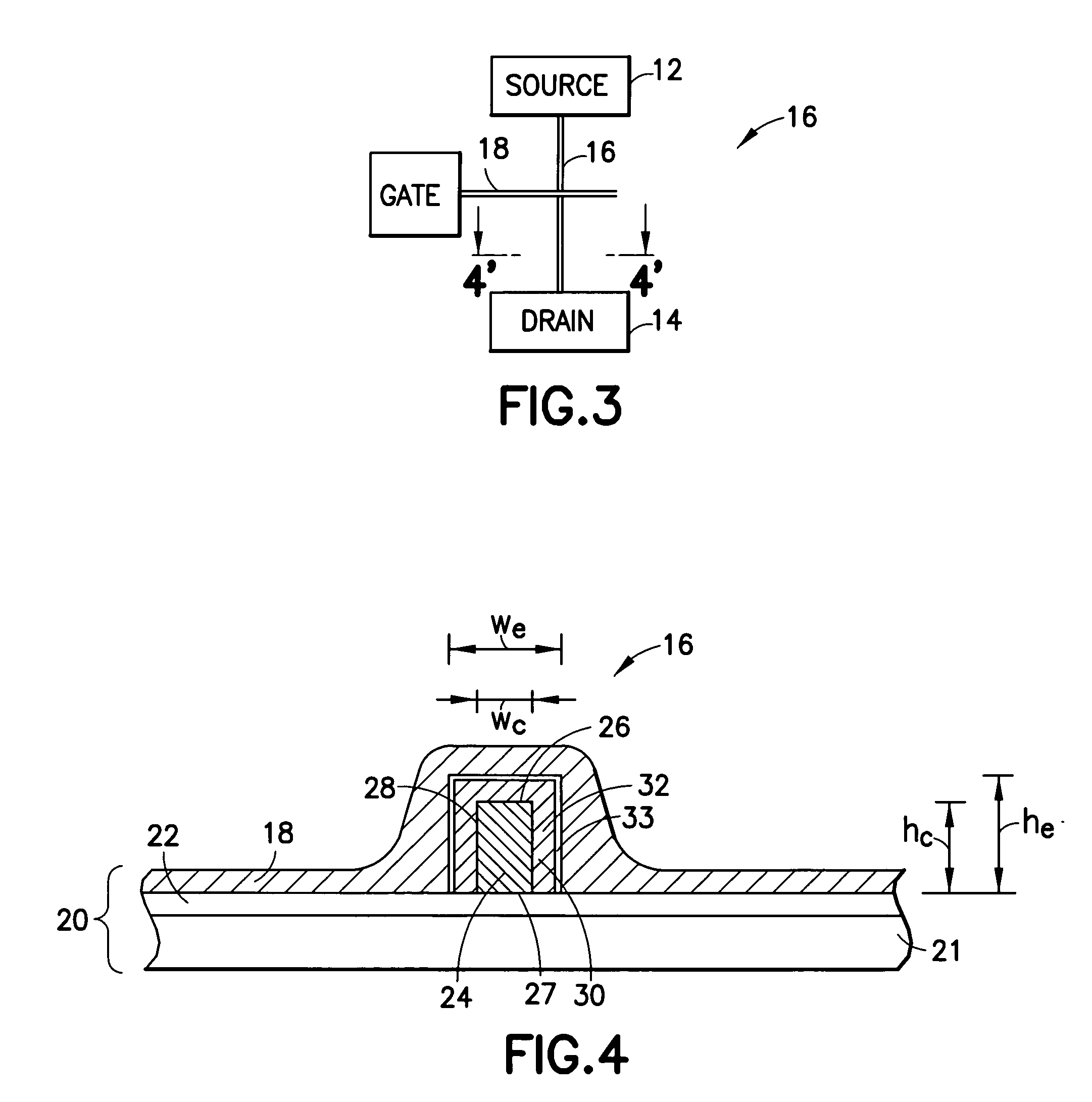
[0010] The foregoing and other problems are overcome, and other advantages are realized, in accordance with the presently preferred embodiments of these teachings. The present invention concerns a channel for electrically connecting a source and a drain of a field effect transistor (FET), commonly called a fin for a FinFET. The channel includes a channel core and a channel envelope. T

Problems solved by technology

Semiconductors and integrated circuit chips have become ubiquitous within many products due to their continually decreasing cost and size.
However, such small scaling necessitates greater control over

Method used


Image

  • FET channel having a strained lattice structure along multiple surfaces
  • FET channel having a strained lattice structure along multiple surfaces
  • FET channel having a strained lattice structure along multiple surfaces

Examples


Example

[0027]FIGS. 1 and 2a-2b are described above and serve as context for understanding the present invention. FIG. 3 depicts in block diagram a FET 10. As known in the art, a source 12 and drain 14 are connected electrically via a channel 16, which is crossed by a gate 18. One or more channels 16 and gates 18 may be present in a single FET 10. As used herein, the length of the channel 16 is the distance from the source 12 to the drain 14 as depicted in FIG. 3.

[0028] A sectional view of the channel 16 at section line 4′-4′ is depicted at FIG. 4. The FET 110 is disposed on a substrate 20 such as silicon 21 overlain with a layer of buried oxide 22. A channel core 24 is made from a first semiconductor material disposed over the substrate 20. The substrate 20 is preferably silicon based, such as a SIMOX wafer, a bonded wafer, or CZ silicon (silicon wafer from the Czochralski process) as known in the art. Preferably, the channel core 24 is formed atop the buried oxide layer 22 that forms par...


PUM


Abstract

A channel 16 of a FinFET 10 has a channel core 24 and a channel envelope 32, each made from a semiconductor material defining a different lattice structure to exploit strained silicon properties. A gate is coupled to the channel envelope through a gate dielectric. Exemplary materials are Si and SixGe1-x, wherein 78<x<92. The channel core 24 has a top surface 26 of width wc and an upstanding surface 28, 30 of height hc, preferably oriented 90° to one another. The channel envelope 32 is in contact with the top 26 and upstanding surfaces 28, 30 so that the area of interface is increased as compared to contact only along the top surface 26, improving electrical conductivity and gate 18 control over the channel 16. The height hc can be tailored to enable a smaller scale FET 10 within a stabilized SRAM. Various methods of making the channel 16 are disclosed, including a mask and etch method, a handle wafer/carrier wafer method, and a shallow trench method. Embodiments and methods for FinFETs with one to four gates are disclosed.

Description

TECHNICAL FIELD [0001] These teachings relate generally to field effect transistors (FET) disposed on a semiconductor wafer or chip, in particular, to a layered structure as a channel that connects a source and a drain of a FET, wherein one of the layers is characterized by a strained lattice structure. BACKGROUND OF THE INVENTION [0002] Semiconductors and integrated circuit chips have become ubiquitous within many products due to their continually decreasing cost and size. Miniaturization in general allows increased performance (more processing per clock cycle and less heat generated) at lower power levels and lower cost. Present technology is at or approaching atomic-level scaling of certain micro-devices such as logic gates, FETs, capacitors, etc. Circuit chips with hundreds of millions of such devices are not uncommon. Further size reductions appear to be approaching the physical limit of trace lines and micro-devices that are embedded upon and within their semiconductor substra...

Claims


Application Information

Patent Timeline
IPC IPC(8): H01LH01L21/336H01L21/8244H01L21/84H01L27/01H01L27/11H01L27/12H01L29/06H01L29/786H01L31/0328H01L31/0336H01L31/072H01L31/109
CPCH01L21/84H01L21/845H01L27/11H01L27/1108H01L27/1203H01L27/1207H01L29/42392H01L29/66795H01L29/785H01L29/78687Y10S257/903H01L27/1211H10B10/00H10B10/125H01L29/04H01L29/7842
Inventor JOSHI, RAJIV V.WILLIAMS, RICHARD Q.
Owner MICROSOFT TECH LICENSING LLC
Why Eureka
Try Eureka