Bipolar transistor and method for producing the same

Inactive Publication Date: 2005-01-27
INFINEON TECH AG
View PDF11 Cites 18 Cited by
  • Summary
  • Abstract
  • Description
  • Claims
  • Application Information

AI Technical Summary

Benefits of technology

[0015] It is a further advantage of the present invention, that the monocrystalline SOI layer on top of the BOX layer can be used as base terminal layer. Apart from saving one process step of the depositing a respective polysilicon layer, as in the conventional bipolar transistor shown in FIG. 3, due to the fact that the base terminal layer is formed of monocrystalline silicon, a realization of significantly lower external base resistors results, which is particularly important for low-noise applications.
[0016] It is another advantage of the present invention that it enables the integration of a vertical bipolar transistor on a thin SOI substrate. Particularly, the silicon layer and the SOI layer, res

Problems solved by technology

When applying bipolar transistors in the analog domain, high demands are made on noiselessness, high-speed and high-frequency capability, respectivel

Method used


Image

  • Bipolar transistor and method for producing the same
  • Bipolar transistor and method for producing the same
  • Bipolar transistor and method for producing the same

Examples


Embodiment Construction

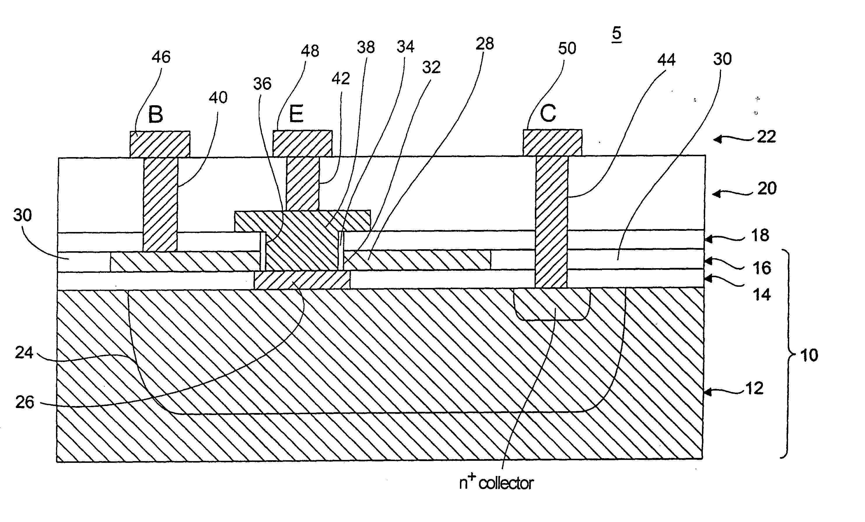
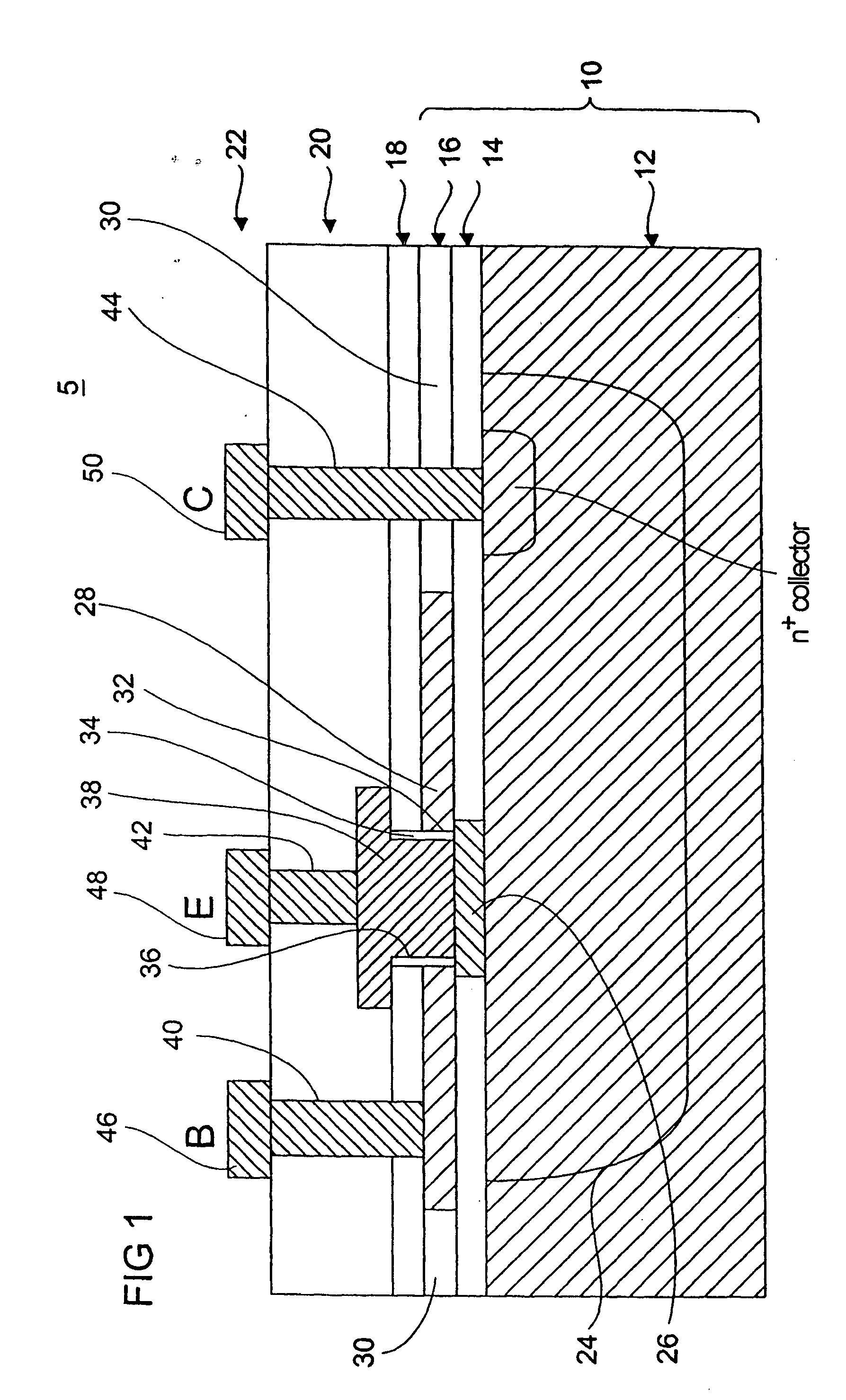
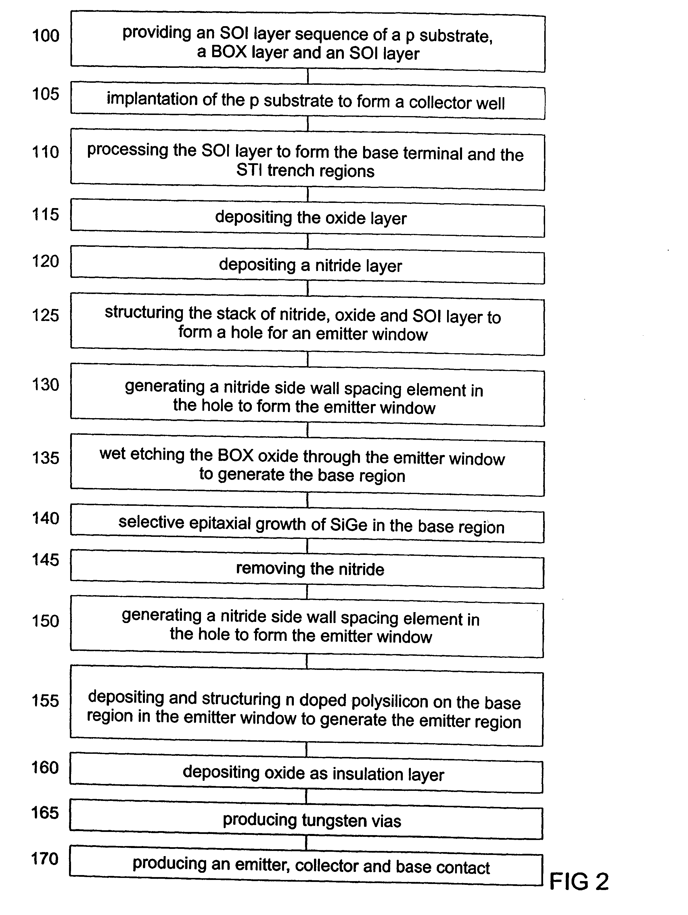
[0022] According to FIG. 1, the structure of a bipolar transistor according to an embodiment of the present invention is described, while its production will be described with reference to FIG. 2.

[0023] The bipolar transistor of FIG. 1 is a vertical bipolar transistor 5 with epitaxial base, which is produced in SOI technique. The bipolar transistor consists mainly of a layer sequence 10, which comprises a p substrate 12, a BOX layer and a first oxide layer 14, respectively, and a SOI layer 16, wherein the BOX layer 14 is disposed between the SOI layer 16 and the p substrate 12. Further, the bipolar transistor 5 comprises a second oxide layer 18 on the SOI layer 16 and an oxide isolation layer 20 on the second oxide layer 18. A structured metal layer 20 is disposed on the isolation layer 20.

[0024] The p substrate serves as transistor substructure. In the p substrate, a doped region of an n collector well 24 is formed. On top of that, an epitaxial Si or SiGe base area and an epitaxi...


PUM


Abstract

A method for producing a bipolar transistor is described, which comprises providing a layer sequence, which comprises a substrate, a first oxide layer and a SOI layer, generating a collector region in the substrate, generating a second oxide layer on the layer sequence, generating a base region in the first oxide layer, such that the base region is in contact with the SOI layer, generating an emitter region on the base region such that the emitter region is isolated from the SOI layer, and generating a collector contact, a base contact and an emitter contact. The present invention is based on the knowledge that the production of a bipolar transistor can be made significantly less expensive when the above layer sequence is used for its production, and thereby, the base region is generated in the BOX layer while the collector region is formed in the substrate. Thereby, otherwise required production process steps and particularly layer deposition steps, such as for a polysilicon or oxide layer, are saved.

Description

CROSS-REFERENCE TO RELATED APPLICATION [0001] This application is a continuation of copending International Application No. PCT / EP02 / 11427, filed Oct. 11, 2002, which designated the United States and was not published in English.BACKGROUND OF THE INVENTION [0002] 1. Field of the Invention [0003] The present invention relates to bipolar transistors and particularly to vertical bipolar transistors in SOI technology as well as the production of the same. [0004] 2. Description of the Prior Art [0005] When applying bipolar transistors in the analog domain, high demands are made on noiselessness, high-speed and high-frequency capability, respectively, and the power consumption of bipolar transistors. Additionally, for cost reduction, there is the desire to be able to produce bipolar transistors via standard methods, such as in CMOS technology (CMOS=complementary metal oxide semiconductor). [0006] In H. Nii, etc., “A 67 GHz fmax Lateral Bipolar Transistor with Co-silicid Base Electrode Str...

Claims


Application Information

Patent Timeline
IPC IPC(8): H01L21/331H01L29/732
CPCH01L29/66287H01L29/66242H01L29/7317H01L29/732
Inventor LACHNER, RUDOLF
Owner INFINEON TECH AG
Why Eureka
Try Eureka