Dynamic random access memory and method of manufacturing the same

a random access memory and dynamic technology, applied in the field of integrated circuits, can solve the problems of difficult burying of barrier layer on the sidewall of word line trenches, affecting the reliability of elements, etc., and achieve good reliability

Active Publication Date: 2022-08-25
WINBOND ELECTRONICS CORP
View PDF3 Cites 0 Cited by
  • Summary
  • Abstract
  • Description
  • Claims
  • Application Information

AI Technical Summary

Benefits of technology

[0007]To sum up, the overhangs formed at the opening end may hinder deposition of the barrier layer, so that it is difficult for the barrier layer to be deposited on the sidewall of the buried word line trench. In this way, after the barrier layer is deposited, the deposition process of doped polysilicon may be directly performed. Since an etching process is not required to be performed, process steps may be saved, and the formed elements may exhibit good reliability.

Problems solved by technology

If there is metal or a barrier layer remaining on the dielectric layer of the sidewall of the buried word line trench when the buried word line is formed, the element reliability problem may occur.
To sum up, the overhangs formed at the opening end may hinder deposition of the barrier layer, so that it is difficult for the barrier layer to be deposited on the sidewall of the buried word line trench.

Method used


Image

  • Dynamic random access memory and method of manufacturing the same
  • Dynamic random access memory and method of manufacturing the same
  • Dynamic random access memory and method of manufacturing the same

Examples


Embodiment Construction

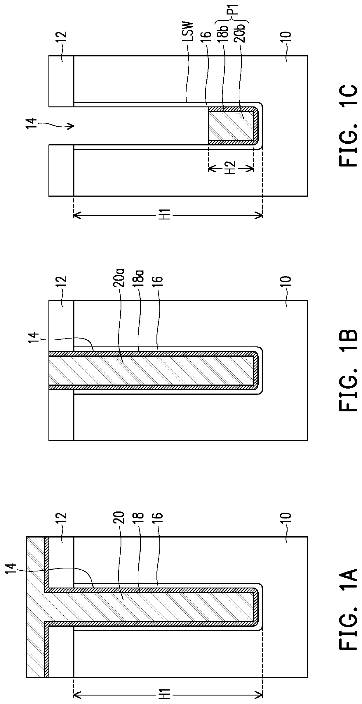
[0010]With reference to FIG. 1A, a substrate 10, such as a silicon substrate, is provided. Next, a hard mask layer 12 having an opening pattern is formed on the substrate 10. The hard mask layer 12 is formed, for example, by forming a hard mask material layer first. Next, the hard mask material layer is patterned through lithography and etching processes. A material of the hard mask material layer is, for example, silicon oxide. The hard mask layer 12 is then treated as a mask to perform an etching process, and a portion of the substrate 10 is removed to form an opening 14. The opening 14 is, for example, a trench, a buried word line trench 14 is treated as an example of the opening 14 for illustration. A depth H1 of the buried word line trench 14 is, for example, 110 nm to 130 nm. An aspect ratio of the buried word line trench 14 is, for example, 3 nm to 10 nm.

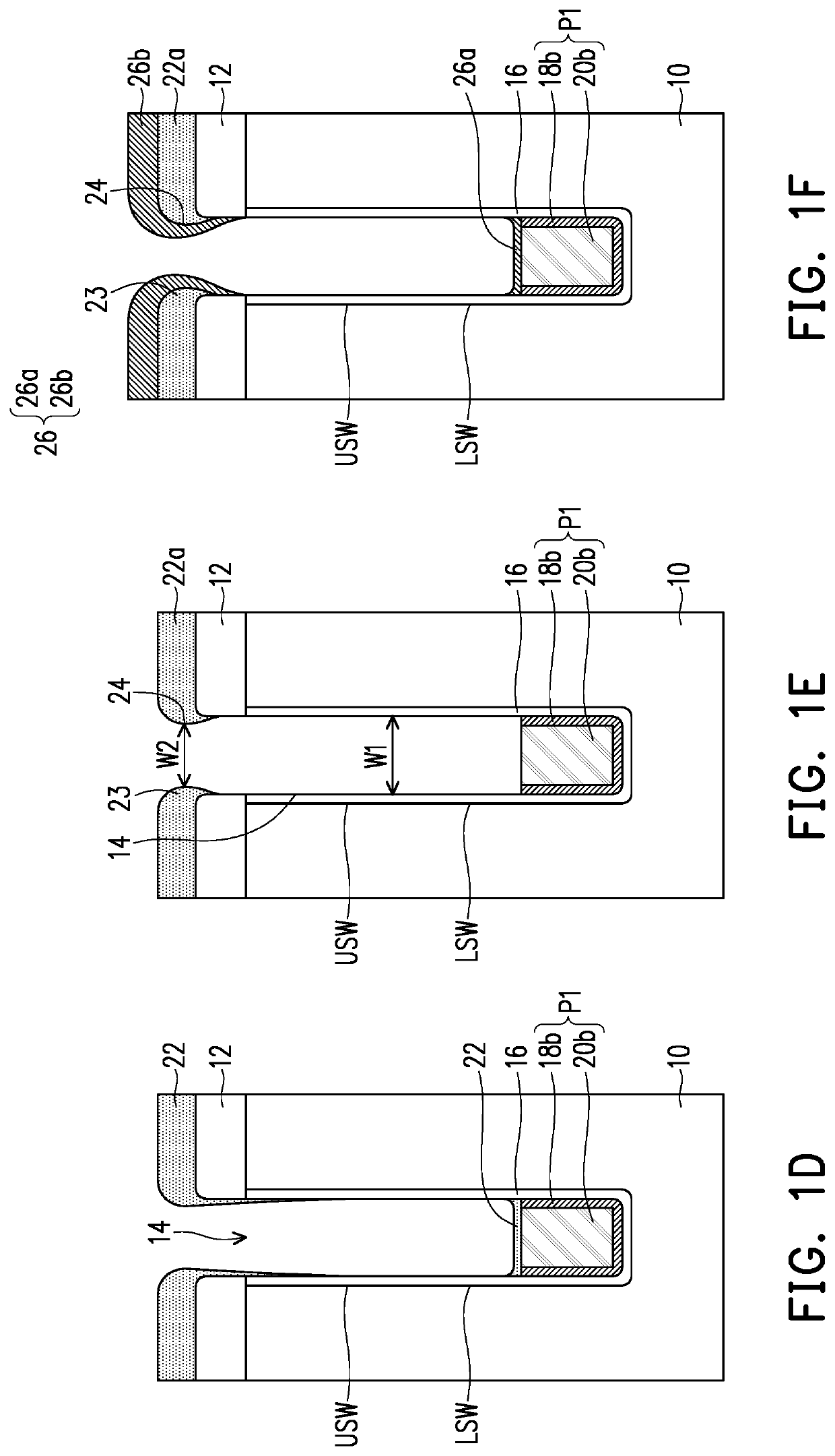
[0011]With reference to FIG. 1A, a dielectric layer 16, a barrier layer 18, and a conductive layer 20 are formed on the har...


PUM

PropertyMeasurementUnit
depth H1aaaaaaaaaa
aspect ratioaaaaaaaaaa
height H2aaaaaaaaaa

Abstract

A method of manufacturing a dynamic random access memory is provided and includes: forming a hard mask layer on a substrate; forming an opening in the hard mask layer and the substrate; forming a dielectric layer on a sidewall of the opening; forming a first part of a buried word line in a lower part of the opening; forming a hard mask layer on a top surface of the hindering layer, where the hindering layer has overhangs covering top corners of the hard mask layer; depositing a first barrier layer on the substrate through hindrance of the overhangs, where the first barrier layer covers the hindering layer and a top surface of the first part and exposes the dielectric layer on the sidewall of the opening; and forming a first conductive layer in the opening, where a sidewall of the first conductive layer contacts the dielectric layer.

Description

CROSS-REFERENCE TO RELATED APPLICATION[0001]This application claims the priority benefit of Taiwan application serial no. 110106821, filed on Feb. 25, 2021. The entirety of the above-mentioned patent application is hereby incorporated by reference herein and made a part of this specification.BACKGROUNDTechnical Field[0002]The disclosure relates to an integrated circuit and a method of manufacturing the same, and in particular, relates to a dynamic random access memory and a method of manufacturing the same.Description of Related Art[0003]As the rapid development of science and technology, in order to meet the requirements of consumers for miniaturized electronic devices, the size of the dynamic random access memory (DRAM) continuously reduces and towards high integration. The buried word line DRAM has been developed in recent years, as element sizes continue to reduce, process margins drop as well. If there is metal or a barrier layer remaining on the dielectric layer of the sidewal...

Claims


Application Information

Patent Timeline
Patent Type & Authority Applications(United States)
IPC IPC(8): H01L27/108H01L21/285H01L21/768H01L21/3213
CPCH01L27/10844H01L21/2855H01L21/76843H01L21/76865H01L21/3213H01L21/76868H01L21/743H01L21/76847H10B12/053H10B12/488H10B12/01
Inventor CHENG, YI-SHENGCHENG, CHIEN-CHANG
Owner WINBOND ELECTRONICS CORP
Why Eureka
Try Eureka