Photomask and integrated circuit manufactured by automatically eliminating design rule violations during construction of a mask layout block

a technology of photomasks and integrated circuits, which is applied in the field of photolithography, can solve the problems of increasing the time needed to design the integrated circuit, layout designers may create design rule violations, and the layout process is complicated, and the disadvantages of eliminating design rule violations on the photomask have been substantially reduced or eliminated

Inactive Publication Date: 2005-01-27
TOPPAN PHOTOMASKS INC
View PDF8 Cites 26 Cited by
  • Summary
  • Abstract
  • Description
  • Claims
  • Application Information

AI Technical Summary

Benefits of technology

[0007] In accordance with the present invention, the disadvantages and problems associated with eliminating design rule violations on a photomask have been substantially reduced or eliminated. In a particular em

Problems solved by technology

The large number of design rules adds complexity to the layout design process because the layout designer may have to memorize or constantly look up the design rules to place polygons in the mask layout database.
Since the process may be completely manual, the layout designer may create design rule violations during the construction of th

Method used


Image

  • Photomask and integrated circuit manufactured by automatically eliminating design rule violations during construction of a mask layout block
  • Photomask and integrated circuit manufactured by automatically eliminating design rule violations during construction of a mask layout block
  • Photomask and integrated circuit manufactured by automatically eliminating design rule violations during construction of a mask layout block

Examples


Embodiment Construction

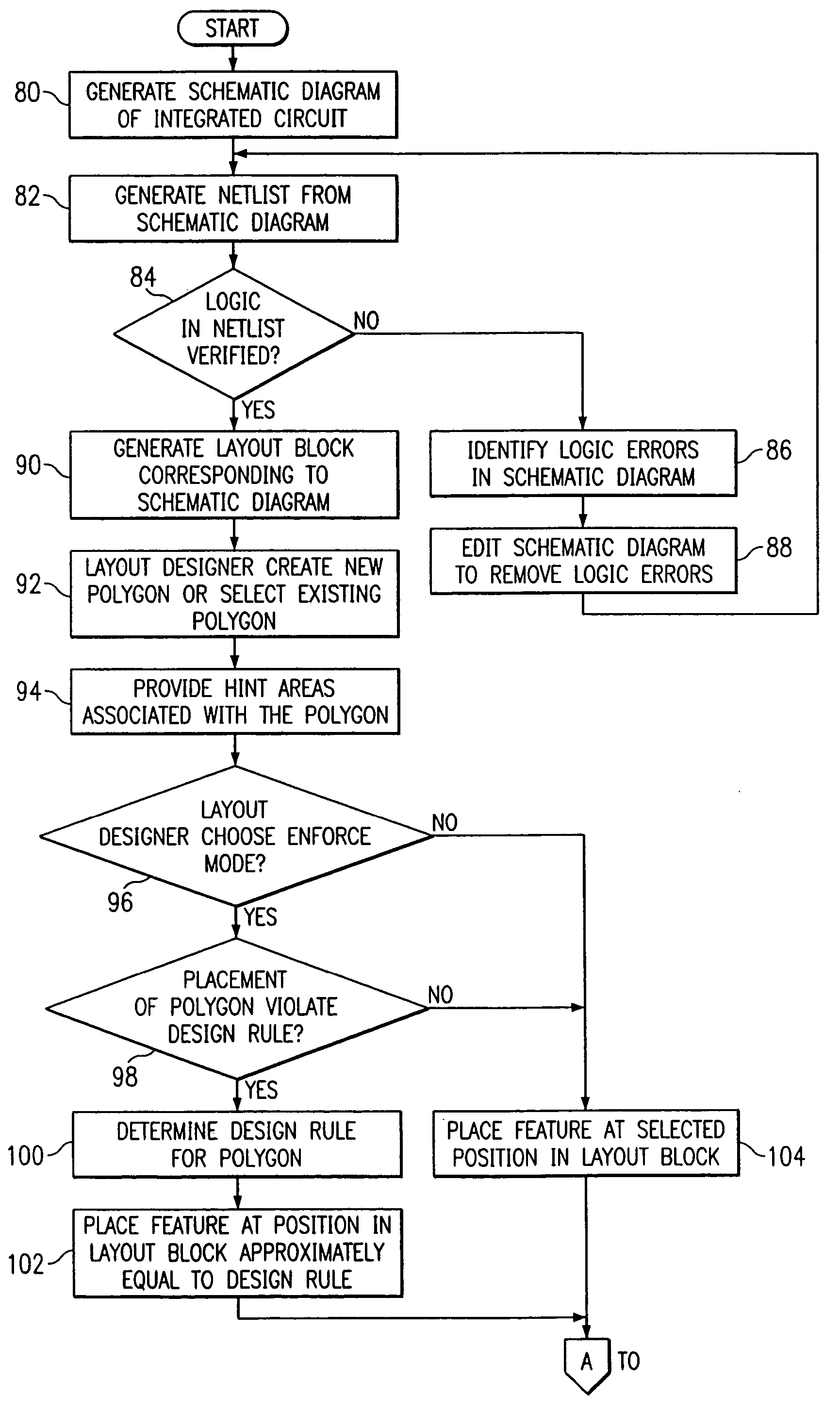
[0020] Preferred embodiments of the invention and its advantages are best understood by reference to FIGS. 1 through 6 of the drawings, like numerals being used for like and corresponding parts of the various drawings.

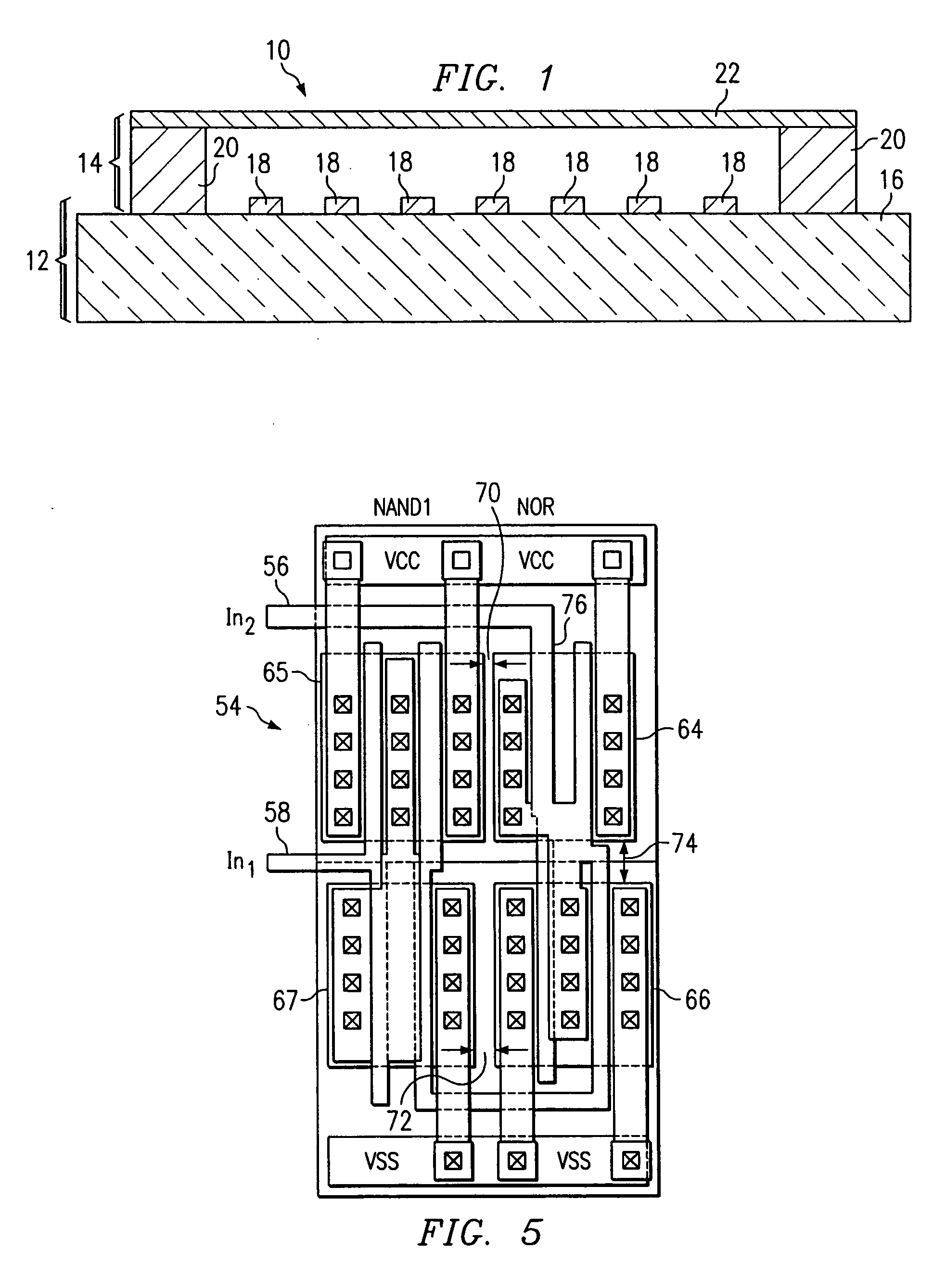
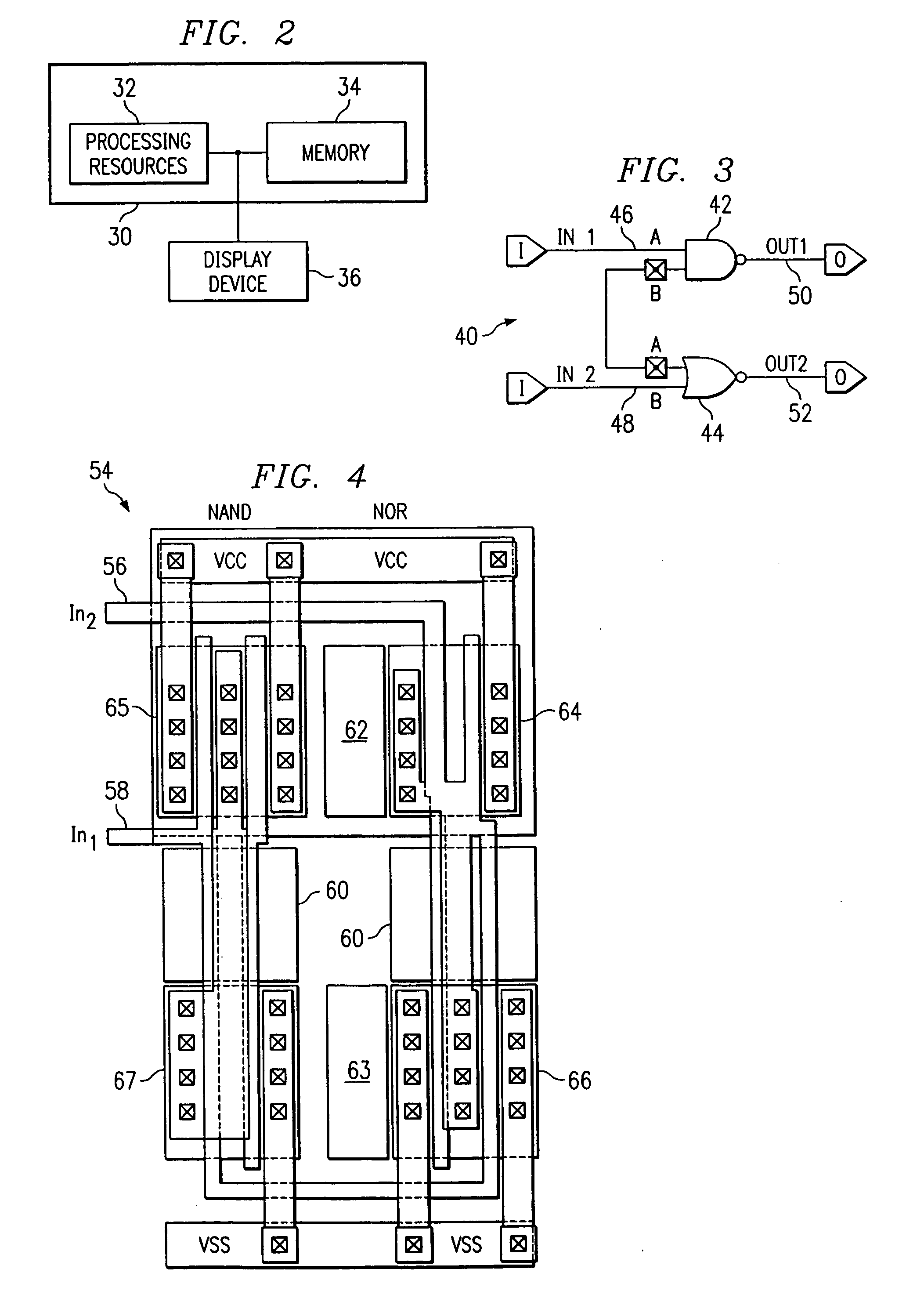
[0021] As the number of transistors on an integrated circuit continues to increase, the design process for the integrated circuit becomes more complex. For example, an increasing number of transistors may require additional layers to form the integrated circuit on a semiconductor wafer. Each layer of the integrated circuit may have one or more design rules that define how polygons on each layer should be placed in a mask layout block for a desired manufacturing process. The number of design rules for the desired manufacturing process, therefore, increases with the number of layers formed on the semiconductor wafer.

[0022] A design rule typically defines the minimum or maximum allowable dimension for a feature fabricated on a specific layer of the integrated circuit. F...


PUM


Abstract

A photomask and integrated circuit manufactured by eliminating design rule violations during construction of a mask layout block are disclosed. A photomask includes a substrate and a patterned layer including at least one feature formed on at least a portion of the substrate. The feature is defined in a mask pattern file generated by analyzing a selected position for a polygon during construction of a mask layout block and determining if the selected position creates a design rule violation in the mask layout block based on a design rule from a technology file. The mask pattern file is further generated by automatically preventing the polygon from being placed in the mask layout block at the selected position if the design rule violation exists.

Description

RELATED APPLICATIONS [0001] This application is a continuation of U.S. patent application Ser. No. 10 / 180,165, filed Jun. 26, 2002 and entitled “PHOTOMASK AND INTEGRATED CIRCUIT MANUFACTURED BY AUTOMATICALLY ELIMINATING DESIGN RULE VIOLATIONS DURING CONSTRUCTION OF A MASK LAYOUT BLOCK,” now U.S. Pat. No. ______; which is a continuation-in-part of U.S. patent application Ser. No. 09 / 634,713, filed Aug. 7, 2000 and entitled “AUTOMATIC DESIGN RULE VIOLATIONS ELIMINATION, WHILE CONSTRUCTING MASK LAYOUT DATABASE (IC LAYOUT), METHOD AND COMPUTER SOFTWARE,” now abandonedTECHNICAL FIELD OF THE INVENTION [0002] This invention relates in general to the field of photolithography, and more particularly to photomask and integrated circuit manufactured by automatically eliminating design rule violations during construction of a mask layout block. BACKGROUND OF THE INVENTION [0003] Over the past several years, the number of transistors in a semiconductor device has increased dramatically. Due to t...

Claims


Application Information

Patent Timeline
IPC IPC(8): G06F17/50
CPCG06F17/5081G06F30/398
Inventor RITTMAN, DANOREN, MICHA
Owner TOPPAN PHOTOMASKS INC
Why Eureka
Try Eureka