

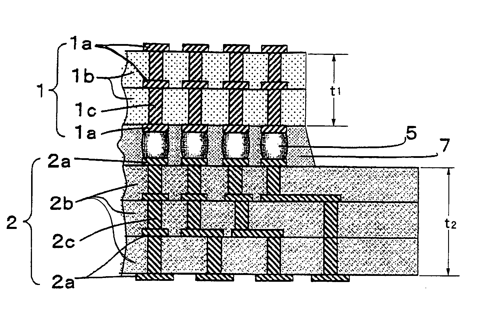
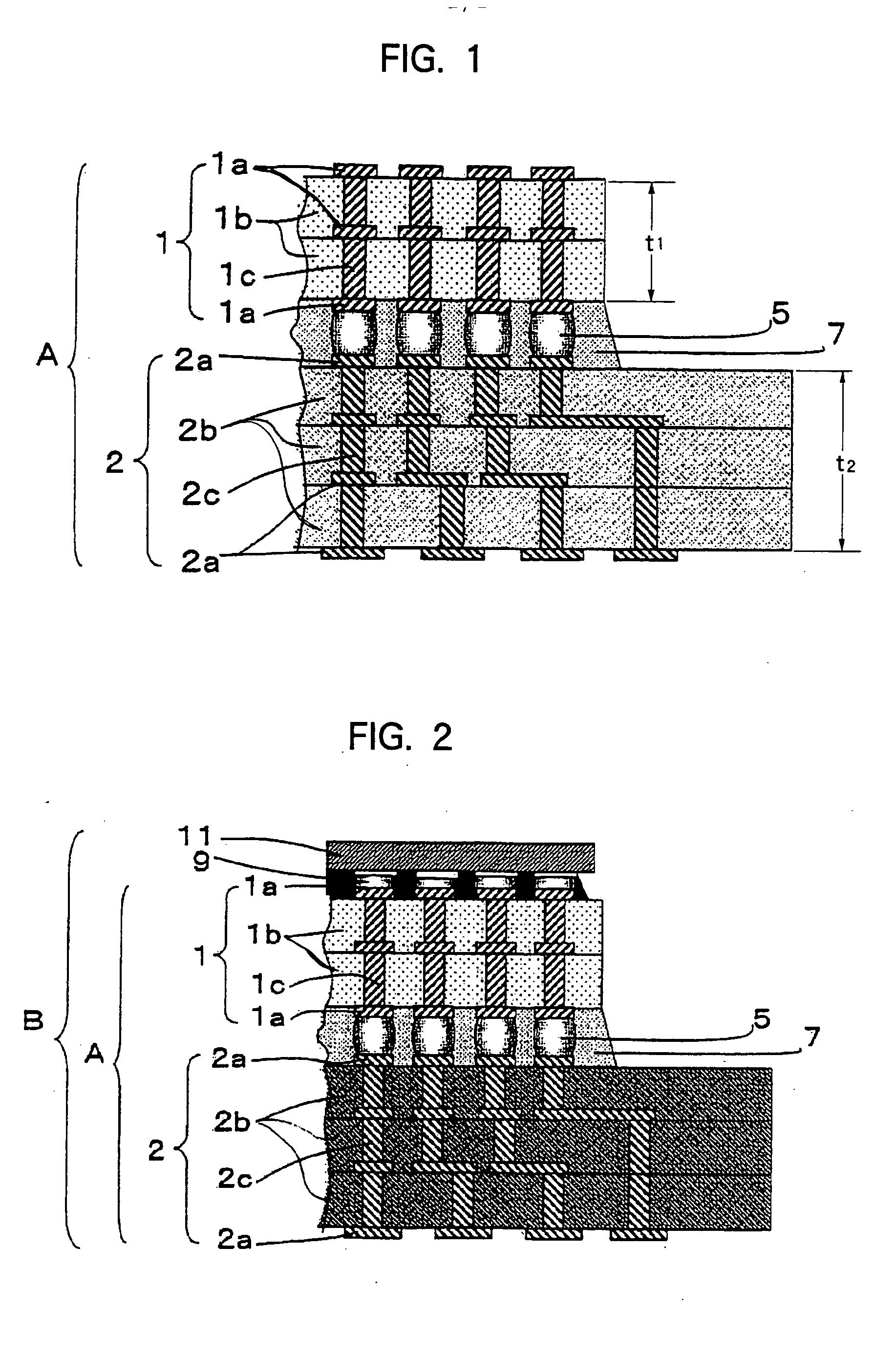
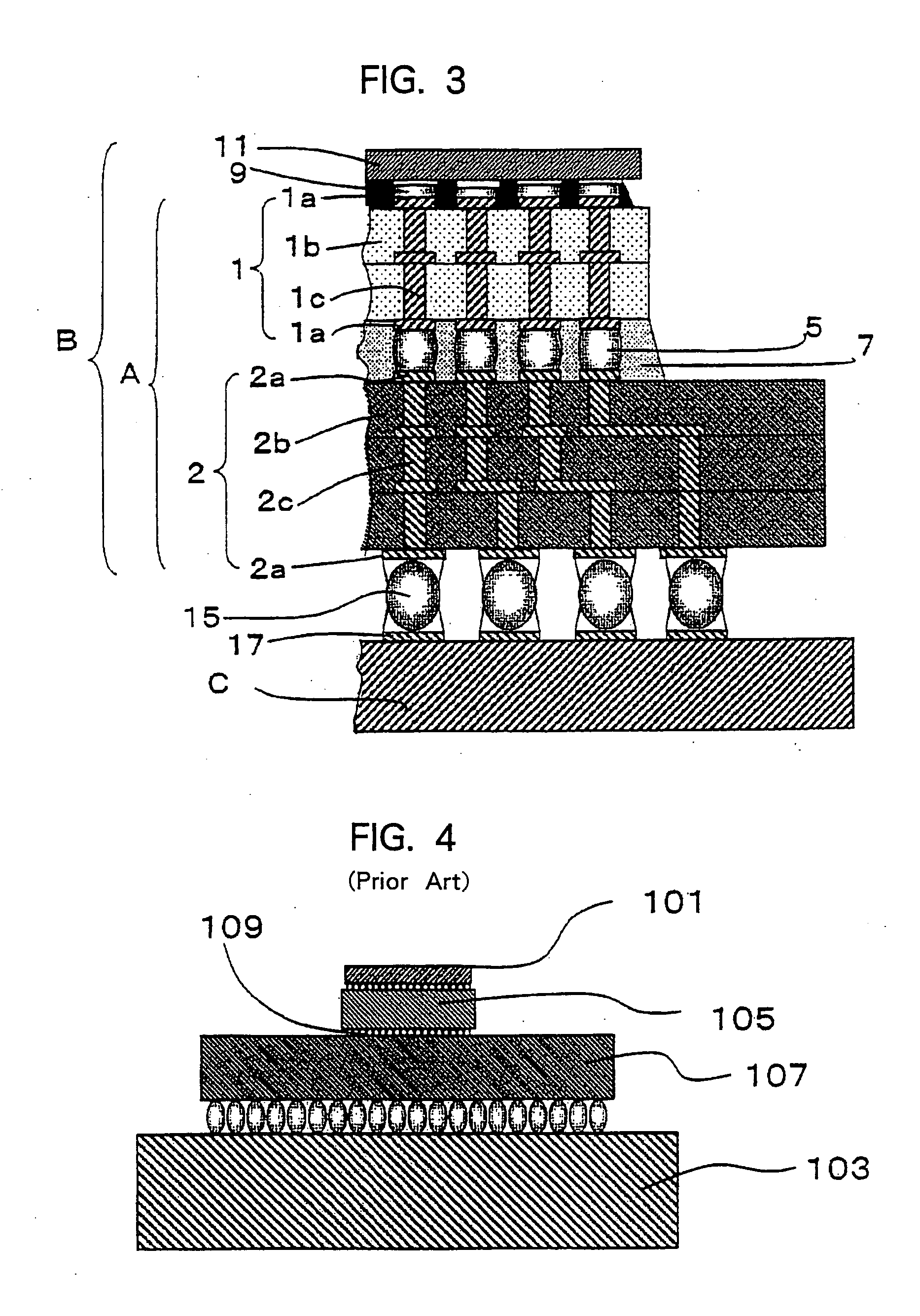
Laminated wiring board and its mounting structure
a technology of mounting structure and wiring board, which is applied in the direction of printed circuit non-printed electric components association, semiconductor/solid-state device details, other domestic articles, etc., can solve the problems of deteriorating the reliability of mounting, reducing mechanical strength, and destroying the solid structure and moving parts due to stress, so as to achieve high reliability and reduce mechanical strength , the effect of high reliability of primary mounting
- Summary
- Abstract
- Description
- Claims
- Application Information
AI Technical Summary
Benefits of technology
Problems solved by technology
Method used
Image

Examples
experiment 1
(Experiment 1)
In order to make sure the effect of the laminated wiring board of the invention, a laminated wiring board for evaluation was prepared as described below.
As insulating materials for forming the first insulated substrate and the second insulated substrate, there were selected a printed substrate having a coefficient of thermal expansion of 16×10−6 / ° C., an alumina substrate having a coefficient of thermal expansion of 5.9×10⁻⁶ / ° C. and glass ceramics A to E shown in Table 1 to prepare first wiring boards (first insulated substrates having a thickness of 0.4 mm and a surface area S1 of 150 mm2) and second wiring boards (second insulated substrates having a thickness of 1 mm and a surface area S2 of 1600 mm2) having properties as shown in Tables 2 and 3.
A eutectic solder paste containing 36 mass % of Pb and 64 mass % of Sn was printed on the wiring layers on the upper surfaces and on the lower surfaces of the first wiring boards and of the second wiring boards by a pr...
experiment 2
(Experiment 2)
First wiring boards (0.4 mm thick) comprising first insulated substrates (GC1 to GC10) having the same wiring layer as that of Experiment 1 and having a thickness of 0.4 mm were obtained by using glasses (G1 go G4) of compositions shown in Table 4 and using filler powders shown in Table 5, and conducting the firing under the conditions shown in Table 5.
There was further prepared a second wiring board (having a thickness of 1 mm and a surface area S2 of 1600 mm2) comprising a second insulated substrate obtained by firing a mixed powder of 50 mass % of a ceramic filler and 50 mass % of a glass powder containing 45 mass % of SiO2, 7 mass % of Al2O3, 13 mass % of B2O3, 12 mass % of CaO and 23 mass % of BaO, and further having the same wiring layer as that of Experiment 1.
The first wiring boards and the second wiring boards were combined as shown in Table 6 to obtain laminated wiring boards in quite the same manner as in Experiment 1. Onto the laminated wiring boards A...
experiment 3
(Experiment 3)
There was prepared a first wiring board comprising a first insulated substrate (GC 12) having a thickness of 4 mm obtained by firing a mixed powder of 28 mass % of a filler powder containing alumina and 72 mass % of a glass powder containing 45 mass % of SiO2, 22 mass % of Al2O3, 18 mass % of MgO, 6 mass % of ZnO and 9 mass % of B2O3, and further having the same wiring layer as that of Experiment 1.
There were further prepared second wiring boards (having an area S2 of 1600 mm2) comprising second insulated substrates (GC21 to GC27) having the same wiring layer as that of Experiment 1 and having a thickness of 1 mm by firing mixed powders of glasses (G21 to G23) of compositions shown in Table 8 and filler powders shown in Table 9.
The first wiring boards and the second wiring boards were combined together as shown in Table 10 to obtain laminated wiring boards A in quite the same manner as in Experiment 1. Onto the laminated wiring boards A were flip chip-mounted (pri...
PUM
| Property | Measurement | Unit |
|---|---|---|
| Temperature | aaaaa | aaaaa |
| Percent by mass | aaaaa | aaaaa |
| Percent by mass | aaaaa | aaaaa |
Abstract
Description
Claims
Application Information