Magnetic random access memory and method of fabricating thereof

a random access memory and magnetic technology, applied in the field of magnetic random access memory devices, can solve the problems of certain microfabrication processing difficulties to be overcom

Active Publication Date: 2005-02-03
INFINEON TECH AG +1
View PDF27 Cites 49 Cited by
  • Summary
  • Abstract
  • Description
  • Claims
  • Application Information

AI Technical Summary

Problems solved by technology

As such, there are certain microfabrication processing difficulties to be overcome before high capacity / density MRAM products become commercially available.
Moreover, magnetic memory elements contain components that are easily oxidized and also sensitive to corrosion.

Method used


Image

  • Magnetic random access memory and method of fabricating thereof
  • Magnetic random access memory and method of fabricating thereof
  • Magnetic random access memory and method of fabricating thereof

Examples


Embodiment Construction

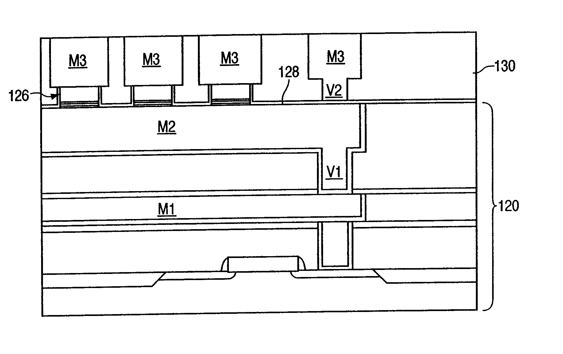
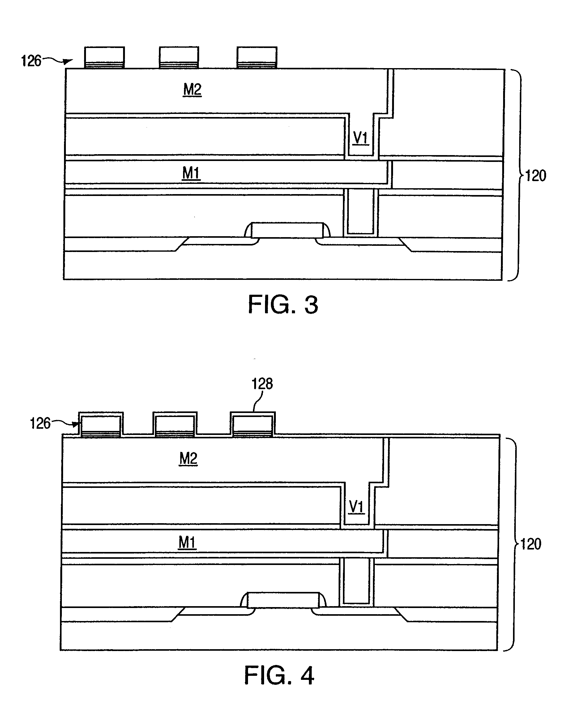
[0012] Disclosed herein is an improved process sequence of fabricating magnetic random access memory (MRAM) devices wherein, among other aspects, a metal hardmask is formed over a plurality of magnetic tunnel junction (MTJ) stacks thereby providing a self-aligned contact between the stacks and subsequent upper metallization lines formed thereupon. The metal hardmask also serves as an etch stop layer for subsequent dual damascene processing steps used in the formation of the upper metallization lines and vias connecting the upper metallization lines to lower metallization lines (on which the MTJ stacks are formed).

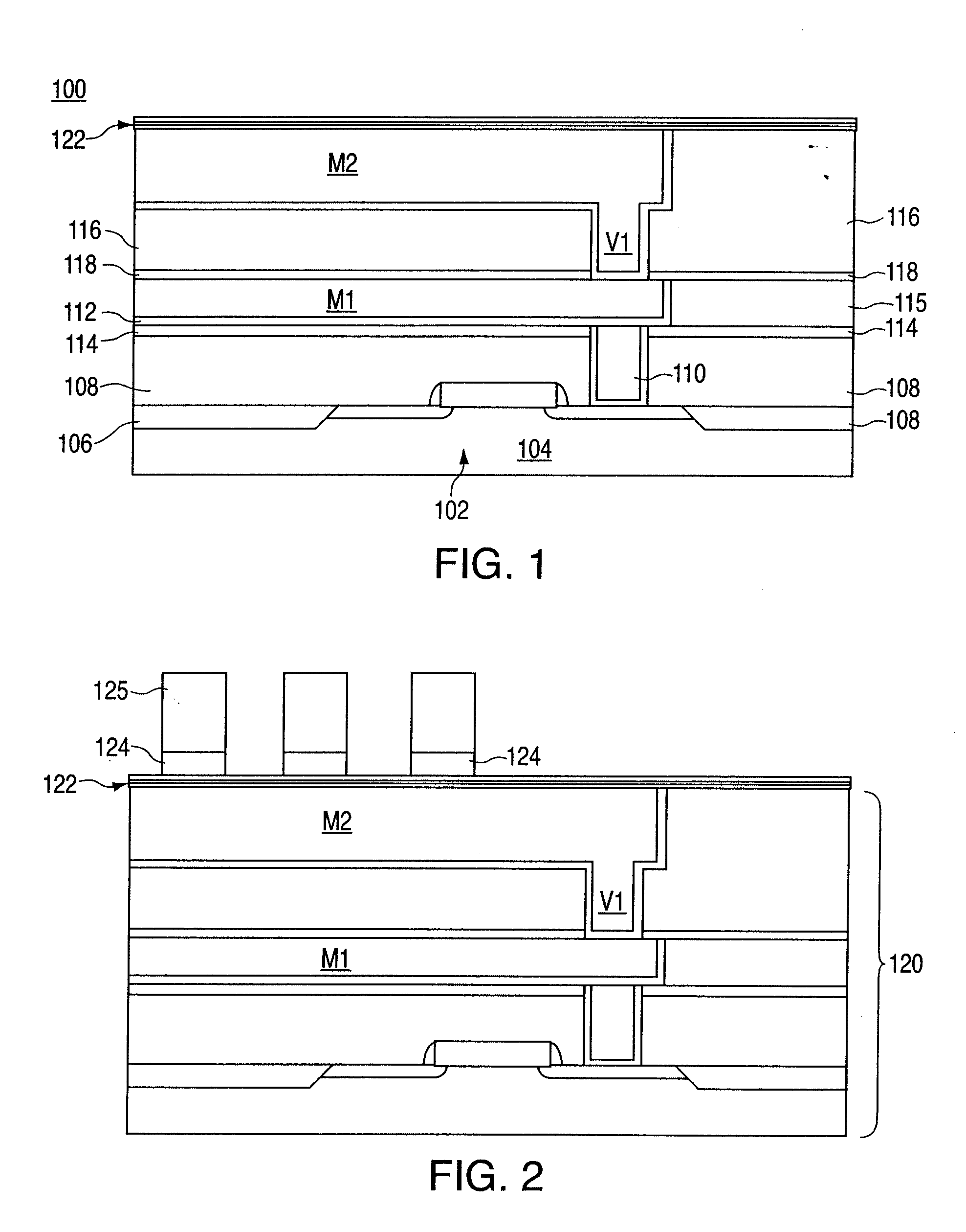
[0013] Referring initially to FIG. 1, there is shown a sectional view of the formation of the MTJ stacks of an MRAM device 100. Prior to the stack formation, the fabrication of the MRAM structure 100, up to the second level of metallization, is implemented in accordance with well known fabrication processes. The lower level, or front end of line (FEOL) structures, include ...


PUM


Abstract

A device structure and method for forming an interconnect structure in a magnetic random access memory (MRAM) device. In an exemplary embodiment, the method includes defining a magnetic stack layer on a lower metallization level, the magnetic stack layer including a non-ferromagnetic layer disposed between a pair of ferromagnetic layers. A conductive hardmask is defined over the magnetic stack layer, and selected portions of the hardmask and the magnetic stack layer, are then removed, thereby creating an array of magnetic tunnel junction (MTJ) stacks. The MTJ stacks include remaining portions of the magnetic stack layer and the hardmask, wherein the hardmask forms a self aligning contact between the magnetic stack layer and an upper metallization level subsequently formed above the MTJ stacks.

Description

BACKGROUND OF INVENTION [0001] The present invention relates generally to magnetic memory devices and, more particularly, to a process sequence of fabricating magnetic random access memory (MRAM) devices. [0002] Magnetic (or magneto-resistive) random access memory (MRAM) is a promising technology in the development of non-volatile random access memory that could begin to replace the existing dynamic random access memory (DRAM) as the standard memory for computing devices. The use of MRAM as a non-volatile RAM will eventually allow for “instant on” systems that come to life as soon as the system is turned on, thus saving the amount of time needed for a conventional PC, for example, to transfer boot data from a hard disk drive to volatile DRAM during system power up. [0003] A magnetic memory element (also referred to as a tunneling magneto-resistive, or TMR device) includes a structure having ferromagnetic layers separated by a non-magnetic layer, and arranged into a magnetic tunnel j...

Claims


Application Information

Patent Timeline
Patent Type & Authority Applications(United States)
IPC IPC(8): G11C11/15H01L21/8246H01L27/22
CPCB82Y10/00H01L27/228G11C11/15H10B61/22
Inventor NUETZEL, JOACHIMNING, XIAN JAYWILLE, WILLIAM C.
Owner INFINEON TECH AG
Why Eureka
Try Eureka