Semiconductor device and manufacturing method thereof

Inactive Publication Date: 2005-02-03
KK TOSHIBA
View PDF9 Cites 35 Cited by
  • Summary
  • Abstract
  • Description
  • Claims
  • Application Information

AI Technical Summary

Benefits of technology

[0019]FIG. 8 is a view showing a relationship between an FT-IR peak height ratio and an

Problems solved by technology

Further, in this type of semiconductor device, a delay in signal transmission becomes one of issues recently.
A problem of this signal transmission delay can be a factor which obstructs an improvement in performance of a semiconductor device.
However, a reactive ion etching (RIE) process which has been adopted as an Al wiring etching technique for a long time cannot be applied to etching of a Cu wiring.
However, the MSQ film has p

Method used


Image

  • Semiconductor device and manufacturing method thereof
  • Semiconductor device and manufacturing method thereof
  • Semiconductor device and manufacturing method thereof

Examples


Embodiment Construction

[0020] An embodiment according to the present invention will be described with reference to the accompanying drawings hereinafter.

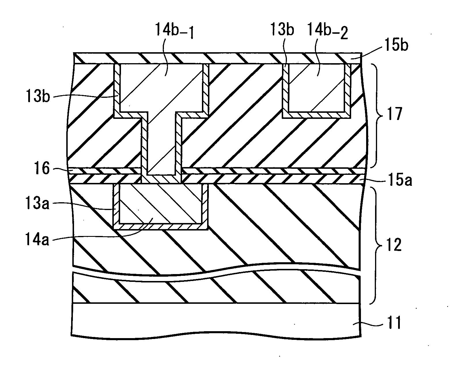
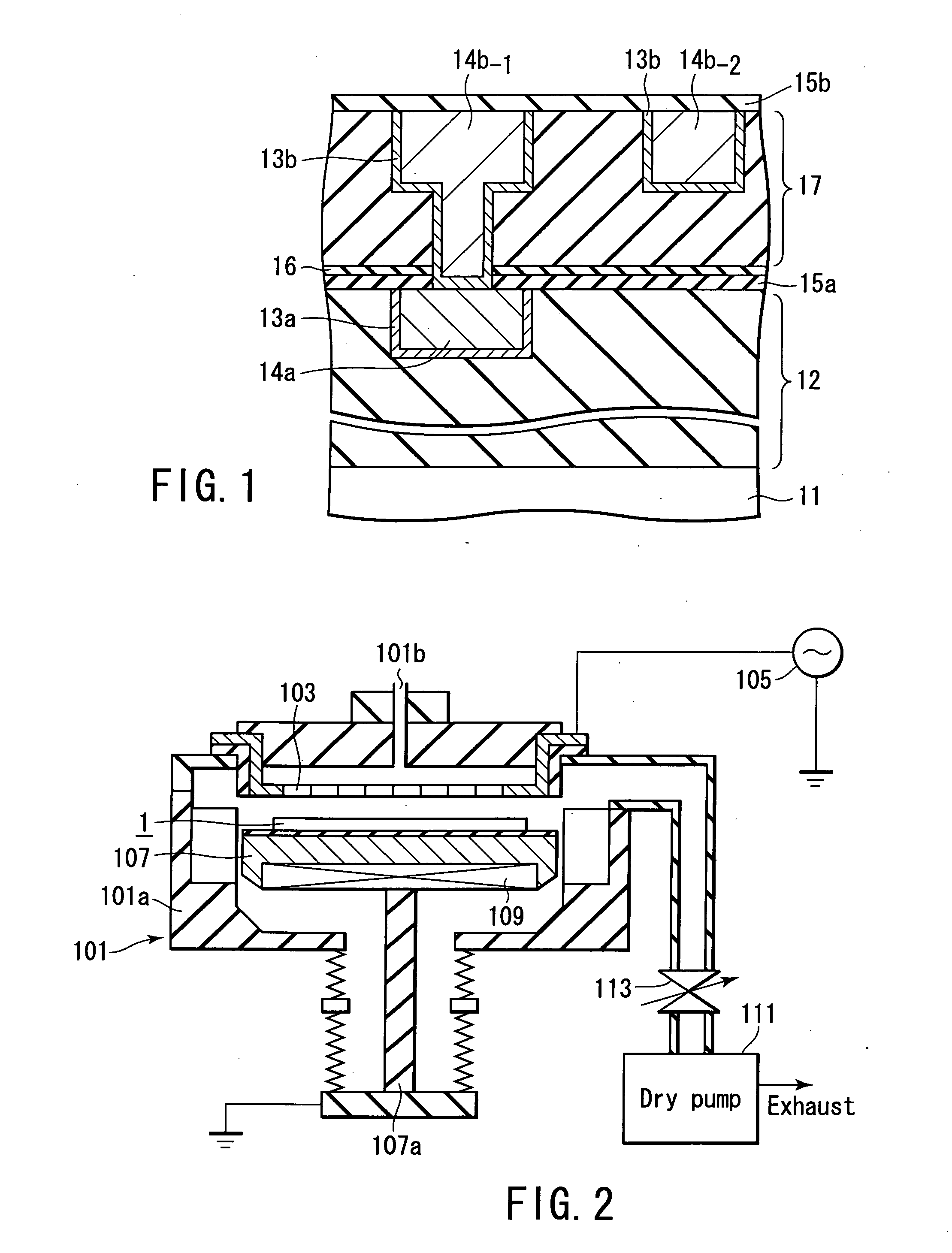
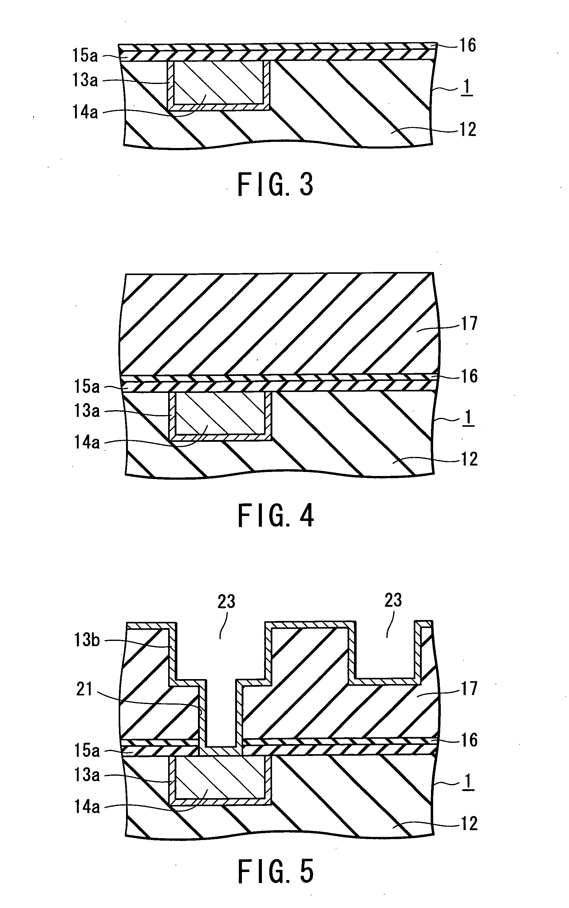
[0021]FIG. 1 shows a basic structure of a semiconductor device according to an embodiment of the present invention. It is to be noted that a semiconductor device having a multilayer wiring structure will be described taking a case that a double layered wiring is provided as an example.

[0022] As shown in FIG. 1, for example, an underlying insulating film 12 is provided on a silicon (which will be abbreviated as an Si hereinafter) substrate 11 having devices formed therein. A first copper (which will be abbreviated as a Cu hereinafter) wiring 14a as a metal wiring of the underlying layer (first layer) is embedded in a part of a surface area of the underlying insulating film 12 accompanying a first barrier metal film 13a. Further, a first methyl radical-containing silicon nitride film (SiCN film) 15a served as an anti-metal diffusion film is provided on th...


PUM


Abstract

A semiconductor device includes a metal wiring provided on a semiconductor substrate. The device further includes an anti-metal diffusion film formed on the metal wiring, a buffer layer which is formed on the anti-metal diffusion film and includes at least a silicon-methyl radical bond and a silicon-oxygen bond, and a low-dielectric constant film layer which is formed on the buffer layer and includes at least the silicon-methyl radical bond and the silicon-oxygen bond, wherein the silicon-methyl radical bonding density of the buffer layer is less than the silicon-methyl radical bonding density of the low-dielectric constant film layer.

Description

CROSS-REFERENCE TO RELATED APPLICATIONS [0001] This application is based upon and claims the benefit of priority from the prior Japanese Patent Application No. 2003-204578, filed Jul. 31, 2003, the entire contents of which are incorporated herein by reference. BACKGROUND OF THE INVENTION [0002] 1. Field of the Invention [0003] The present invention relates to a semiconductor device and a manufacturing method thereof. More particularly, the present invention relates to formation of a low-dielectric constant silicon oxide film by a plasma chemical vapor deposition (CVD) method on a semiconductor substrate in process. [0004] 2. Description of the Related Art [0005] Conventionally, in a semiconductor device, a silicon oxide (SiO2) film is often used as an insulating film utilized to electrically isolate between wirings in a device. This SiO2 film is mainly formed by a low pressure or atmospheric pressure CVD method using such as SiH4 or tetraethoxysilane (TEOS) as a source gas. In parti...

Claims


Application Information

Patent Timeline
IPC IPC(8): H01L21/312H01L21/316H01L21/768H01L23/522H01L23/532
CPCH01L21/3124H01L21/3125H01L21/76807H01L21/76832H01L21/76834H01L21/76835H01L2924/0002H01L23/53238H01L23/53295H01L2924/00H01L21/02274H01L21/02304H01L21/02126H01L21/02137H01L21/02211
Inventor WATANABE, KEINAGAMATSU, TAKAHITO
Owner KK TOSHIBA
Why Eureka
Try Eureka