Solventless thermosetting photosensitive via-filling material

a photosensitive via-filling and thermosetting technology, applied in the direction of photosensitive materials, auxiliary/base layers of photosensitive materials, instruments, etc., can solve the problems of complex via-filling process, broken signal transmission, and product uselessness

Inactive Publication Date: 2005-02-03
YEH TODD
View PDF24 Cites 23 Cited by
  • Summary
  • Abstract
  • Description
  • Claims
  • Application Information

AI Technical Summary

Benefits of technology

[0016] one or more epoxy resin curing agents.
[0017] Furthermore, the solventless thermosetting photosensitive via-filling material comprises one or more optional inorganic fillers for adjusting physical properties thereof such as electrical insulation, acid resistance, Theological properties, etc.; and one or more optional organic adjuvants for achieving desired processing characteristics for the via-filling step.
[0018] For more detailed information regarding advantages and features of the present invention, examples of preferred embodiments will be described below with reference to the annexed drawings.

Problems solved by technology

Without the via-filling material, the connector within via is subjected to oxidation by air trapped therein, which in turn leads to breaking of signal transmission and renders the product useless.
Though it seems simple, via-filling process is complicated.
Sometimes, it is really a challenging step.
Generally speaking, problems encountered are such as bubbles inside the filling, volcanoes on the surface and recessed or bulged filling surface profiles along the plane of circuit patterns.
Until now, the industry-wise yield-rate of this step is still far from satisfactory.
However, smooth surface is difficult to acquire in practice.
Since the solvent content for most commercial solder resistant products is relatively high, i.e. up to 25%, which results in voids or recessed surfaces.
Such problems are due to evaporation of solvent in the subsequent baking process.
The via-filling material shrinks as the loss of the volume of solvent, thus results in recessed surfaces or voids.
Therefore, the existence of solvent is detrimental to the via-filling process.
Unfortunately, current commercial via-filling products still contain certain problems, so that the yield rate is largely limited.
Sagging is a common problem, which is the flowing of the filling material out of via during the curing process.
As a result, the lack of coverage of the filling material along the top edge of via and excessive coverage along the bottom edge of via forms.

Method used


Image

  • Solventless thermosetting photosensitive via-filling material
  • Solventless thermosetting photosensitive via-filling material
  • Solventless thermosetting photosensitive via-filling material

Examples


example 1

[0041] A solventless thermosetting photosensitive via-filling material consists of 100 parts by weight bisphenol-A epoxy resins (LG N-730), 6 parts by weight 2,4-diamino-6[2′-methylimidazoly-(1′)] ethyl-S-triazine isocyanuric acid addition compound, 20 parts by weight tris(2-hydroxyethyl) isocyanurate triacrylate, 2 parts by weight 2-methyl-1-[4-(methylthio)phenyl]-2-morpholinopropanone, 0.2 parts by weight 2-isopropyl thioxanthone, 2.5 parts by weight Aerosil R974 and 3 parts by weight Defoamer KS-66.

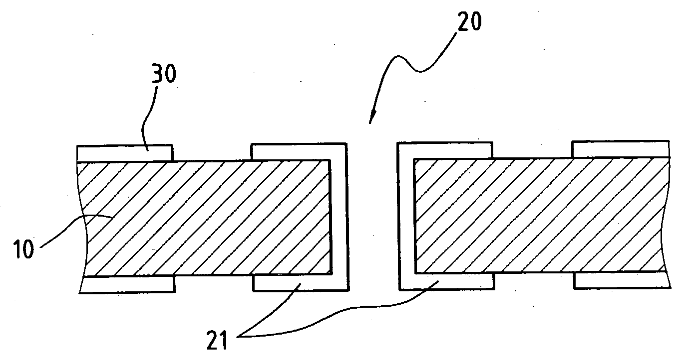
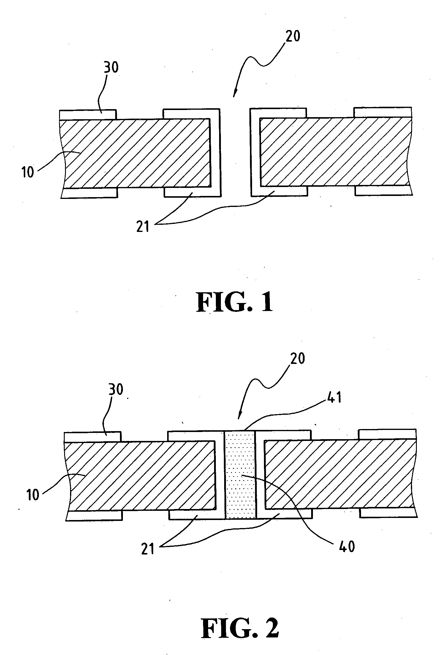
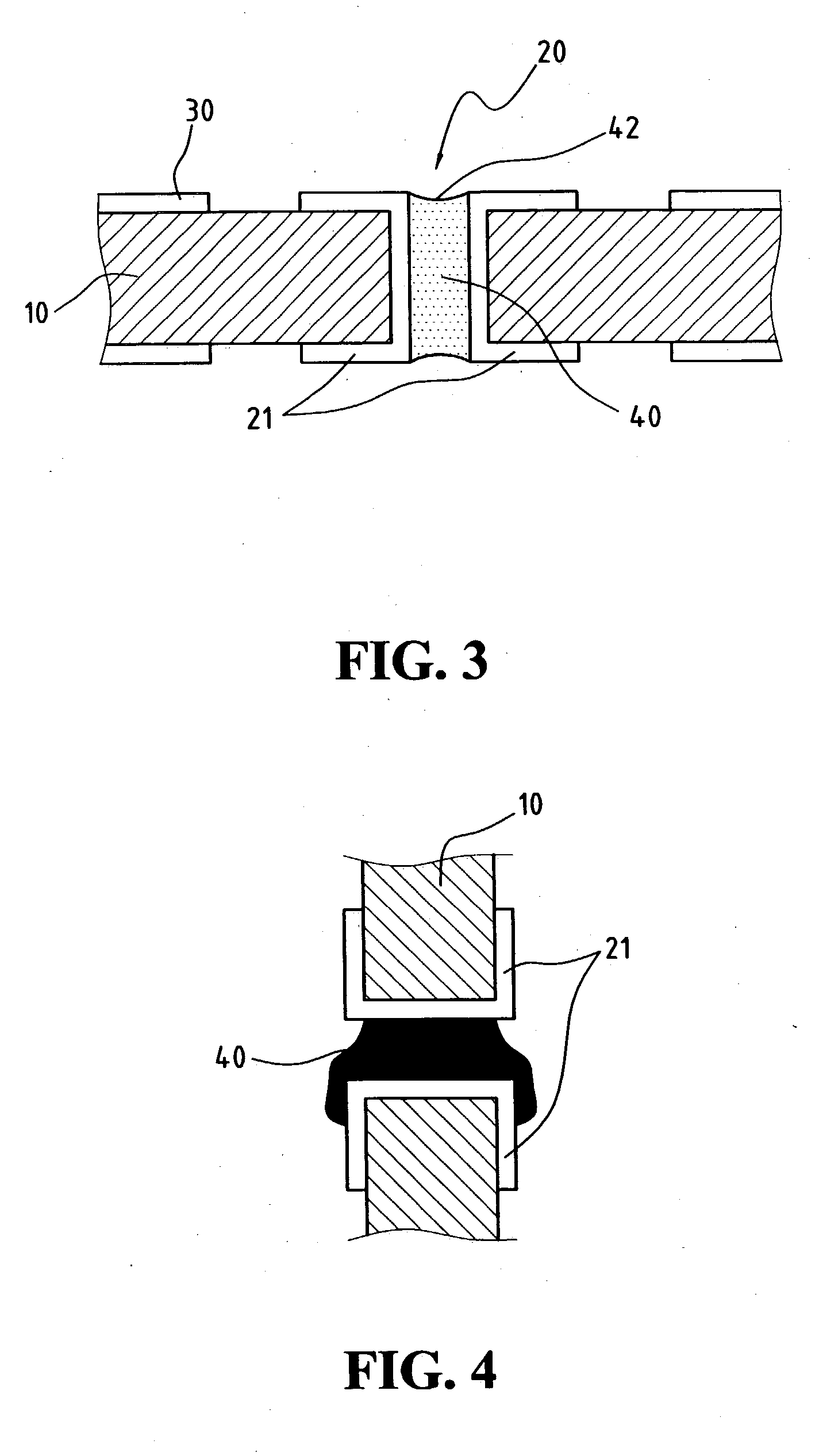
[0042] The solventless thermosetting photosensitive via-filling material is used to fill up the via by screen printing on PCB. Then, the PCB is mounted in a 7 kW ultraviolet exposure machine for a short-time exposure with exposure energy of 1 mJ / cm2. As a result, solid barrier films with a thickness of greater than 50 μm form at both ends of the via-filling material. The solid barrier films will prevent the internal solventless thermosetting photosensitive material from flowing out of...

example 2

[0044] A solventless thermosetting photosensitive via-filling material consists of 100 parts by weight bisphenol-F epoxy resins (Epon-862), 6 parts by weight 2,4-diamino-6[2′-methylimidazoly-(1′)] ethyl-S-triazine isocyanuric acid addition compound, 15 parts by weight trimethylolpropane triacrylate, 2 parts by weight 2-methyl-1-[4-(methylthio)phenyl]-2-morpholinopropanone, 0.2 parts by weight 2-isopropyl thioxanthone, 2.5 parts by weight Aerosil R974 and 3 parts by weight Defoamer KS-66.

[0045] The solventless thermosetting photosensitive via-filling material is used to fill up the via by screen printing on PCB. Then, the PCB is mounted in a 7 kW ultraviolet exposure machine for a short-time exposure with exposure energy of 1 mJ / cm2. As a result, solid barrier films with a thickness of greater than 50 μm form at both ends of the via-filling material. The solid barrier films prevent the internal solventless thermosetting photosensitive material from flowing out of via.

[0046] After u...


PUM

PropertyMeasurementUnit
temperatureaaaaaaaaaa
thicknessaaaaaaaaaa
temperatureaaaaaaaaaa

Abstract

A via-filling material improves a via-filling process in manufacturing multi-layered printed circuit boards. The via-filling material is capable of undergoing UV pre-cure and thermal post-cure step. Exposed to ultraviolet light, the via-filling material filled up the two ends of the via form solid barrier films so that the inside via-filling material will not flow out during a thermal post curing process due to an lower viscosity of said material. The dual-cure treatment resolves the problems of polishing, sagging and bubbling in the via-filling process and ensures the integrity of the filling material. As a result, the via-filling material with smooth surface and a solid inside without void or hole therein formed.

Description

BACKGROUND OF THE INVENTION [0001] 1. Field of the Invention [0002] The present invention relates to thermosetting photosensitive material, and specifically to a thermosetting photosensitive material for via-filling process in manufacturing printed circuit boards. [0003] 2. The Prior Arts [0004] In recent years, owing to the surging demands of mobile phones, personal electronic organizers and laptops, consumers are increasingly demanding electronic products lighter, thinner, and smaller. The printed-circuit-board (PCB) industry, which has to support the electronic industries in their development, are also pushed towards manufacturing processes that are capable of handling this trend. To make lighter, thinner, and smaller electronic products, people pack more circuit density onto the ever-decreasing board area, or so-called high-density-integration. The technology of multi-layered boards manufacturing also plays an essential role in the revolution towards high-density-integration. [0...

Claims


Application Information

Patent Timeline
Patent Type & Authority Applications(United States)
IPC IPC(8): G03C1/76G03F7/032G03F7/038H05K3/00H05K3/46
CPCG03F7/032G03F7/038H05K2201/0959H05K3/4602H05K3/0094C09D4/06C08F283/06
Inventor YEH, TODD
Owner YEH TODD
Why Eureka
Try Eureka