
Superconducting circuit

a superconducting circuit and circuit technology, applied in the direction of superconductor devices, electrical apparatus, semiconductor devices, etc., can solve the problems of hysteresis of the junction of the sfq circuit, inability to display the maximum performance, and inability to display the rapidness, etc., to achieve high performance

Inactive Publication Date: 2005-02-10
FUJITSU LTD +1
View PDF1 Cites 8 Cited by
  • Summary
  • Abstract
  • Description
  • Claims
  • Application Information

AI Technical Summary

Benefits of technology

[0010] The present invention has been carried out in consideration of the above-described disadvantage, and the present invention is to provide a superconducting circuit which widen an operational region where a single flux quantum circuit and an interface circuit can operate coexistingly in an operation of the super conducting circuit provided with the single flux quantum circuit using the high temperature superconductor and an interface circuit, so that respective circuits can exhibit operations in high performance.

Problems solved by technology

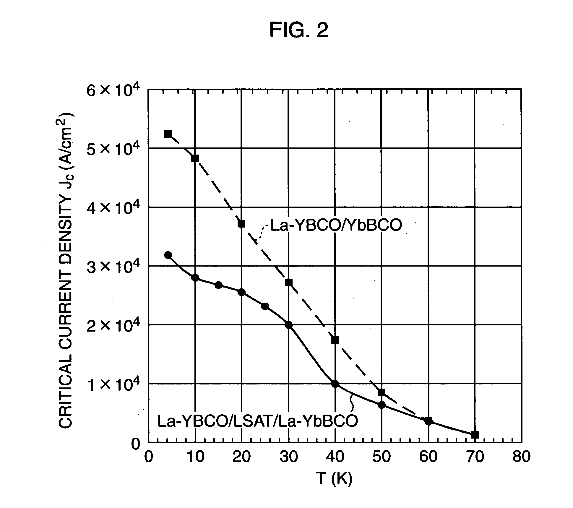
However, since in the above-described superconducting circuit, for both of the SFQ circuit and the interface circuit, operation has to be carried out in a slight operational region in which the SFQ circuit and the interface circuit can coexist respectively, there has been a disadvantage that respective maximum performances, for instance, rapidness cannot be displayed.
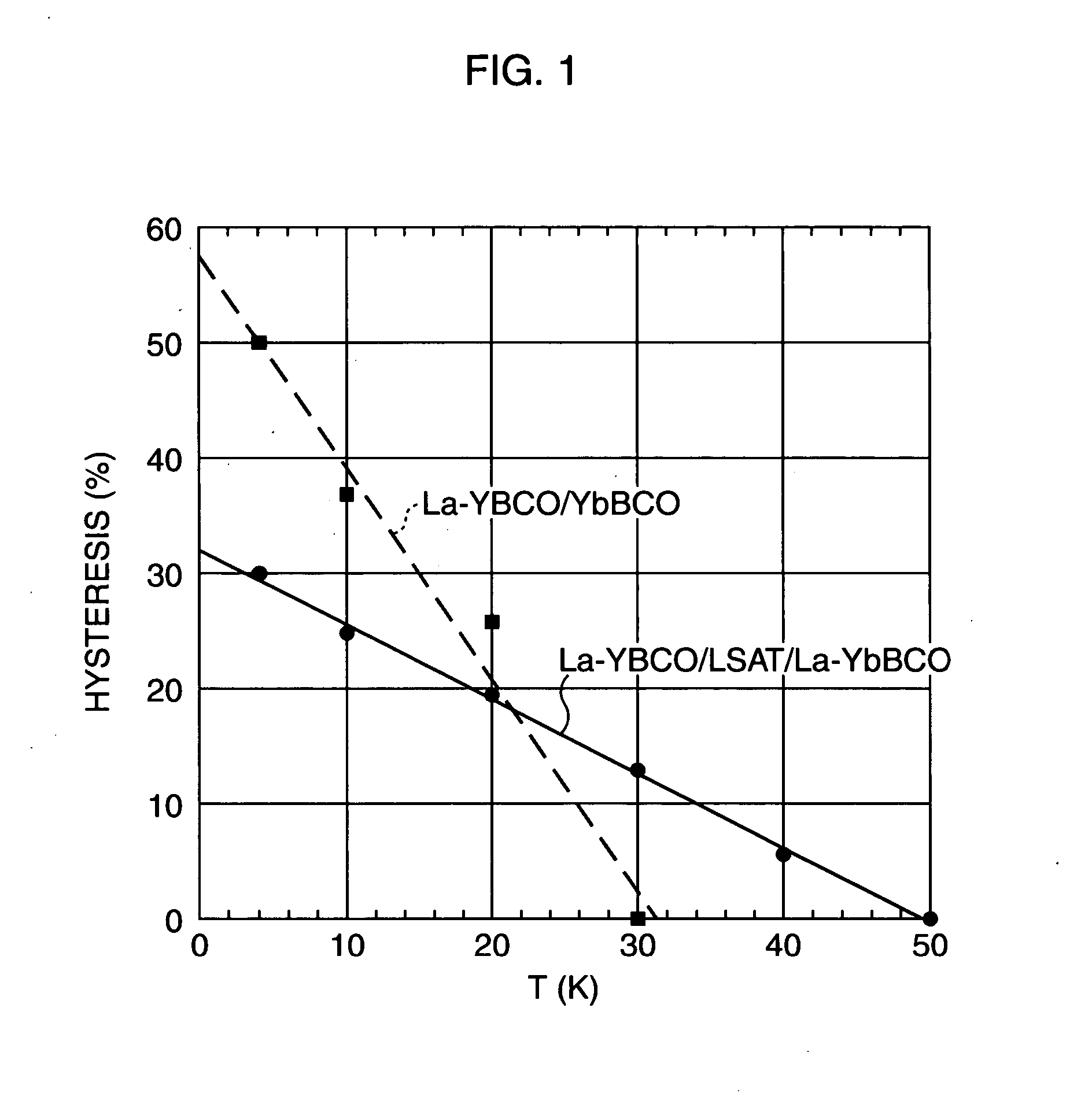
For instance, in order to improve the performance of the interface circuit, when the critical current density is set larger than the operational region, junction of the SFQ circuit also exhibits hysteresis, which makes operation of the SFQ circuit impossible.
On the other hand, in order to improve the performance of the SFQ circuit, when the critical current density is set smaller than the operational region, the junction of the interface circuit loses hysteresis necessary for its own operation, which makes operation of the interface circuit impossible.

Method used


Image

  • Superconducting circuit
  • Superconducting circuit
  • Superconducting circuit

Examples


embodiment adopting

[0032] Concrete Embodiment Adopting Gist of Present Invention

[0033] Next, various embodiments based on the gist of the superconducting circuit of the present invention will be described. Further, an example of adopting a latch driver circuit as an interface circuit of the superconducting circuit in an embodiment of the present invention will be explained.

first embodiment

[0034] First Embodiment

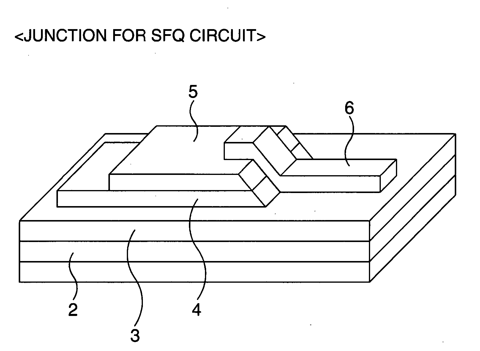
[0035]FIGS. 4A and 4B are perspective views showing configurations of junction parts of an SFQ circuit and a latch driver circuit in a superconducting circuit in a first embodiment.

[0036] A junction part of the SFQ circuit shown in FIG. 4A is formed of a lower electrode 4 made from lantern (La)-doped YBaCuO of about 200 nm in thickness, an insulating layer 5 made from SrSnO of about 300 nm in thickness on the lower electrode 4, and an upper electrode 6 made from YbBaCuO of about 200 nm in thickness on ramp edges of the insulating layer 5 and the lower electrode 4. At the ramp edges of the insulating layer 5 and the lower electrode 4, a damage layers (not shown) to be served as a barrier is formed by ion milling with Ar or the like.

[0037] On the other hand, the junction part of the latch driver circuit shown in FIG. 4B is formed of a lower electrode 12 made from La-doped YBaCuO of about 200 nm in thickness, an insulating layer 13 made from SrSnO of about 300 ...

second embodiment

[0039] Second Embodiment

[0040]FIG. 5A and FIG. 5B are perspective views showing configurations of junction parts of an SFQ circuit and a latch driver circuit in a superconducting circuit in the second embodiment.

[0041] The junction part of the SFQ circuit shown in FIG. 5A is formed of a lower electrode 4 made from La-doped YBaCuO of about 200 nm in thickness, an insulating layer 5 made from SrSnO of about 300 nm in thickness on the lower electrode 4, and an upper electrode 26 made from La-doped YbBaCuO of about 200 nm in thickness on ramp edges of the insulating layer 5 and the lower electrode 4. At the ramp edges of the insulating layer 5 and the lower electrode 4, a damage layer (not shown) serving as a barrier is formed by ion milling with Ar or the like.

[0042] On the other hand, the junction part of the latch driver circuit shown in FIG. 5B is, similarly to the junction part of the latch driver circuit in the first embodiment, formed of a lower electrode 12 made from La-doped ...


PUM


Abstract

A first Josephson junction in a Single Flux Quantum circuit (SFQ circuit) and a second Josephson junction in an interface circuit (latch driver circuit) are formed with junction materials different from each other, and the junction materials are selected so that the hysteresis of the first Josephson junction in a current-voltage characteristic is smaller than the hysteresis of the second Josephson junction in a current-voltage characteristic.

Description

CROSS-REFERENCE TO RELATED APPLICATIONS [0001] This application is based upon and claims the benefit of priority from the prior Japanese Patent Application No. 2003-092545, filed on Mar. 28, 2003, the entire contents of which are incorporated herein by reference. BACKGROUND OF THE INVENTION [0002] 1. Field of the Invention [0003] The present invention relates to a superconducting circuit provided with a Single Flux Quantum (SFQ) circuit using a high temperature superconductor and an interface circuit for the single flux quantum circuit, and is applicable to fields of communication, computing, and instrumentation such as routers for communication, servers, AD converters, samplers, and so on. [0004] 2. Description of the Related Art [0005] Conventionally, high temperature superconductor junctions have been thought to be applicable to the SFQ circuits as they are without being shunted by resistance because their current-voltage characteristics are called an overdamp type, and unlike lo...

Claims


Application Information

Patent Timeline
IPC IPC(8): H01L27/18H01L39/22
CPCH01L39/225H01L27/18H10N69/00H10N60/124
Inventor HATO, TSUNEHIROHORIBE, MASAHIROTANABE, KEIICHI
Owner FUJITSU LTD
Learn More