Structure and method of making strained semiconductor CMOS transistors having lattice-mismatched source and drain regions

a technology of strained semiconductors and drain regions, applied in the direction of transistors, crystal growth processes, chemistry apparatus and processes, etc., can solve the problems of difficult to obtain holes and improve the mobility of holes, and the performance declines

Inactive Publication Date: 2005-02-10
SEMICON MFG INT (SHANGHAI) CORP
View PDF2 Cites 150 Cited by
  • Summary
  • Abstract
  • Description
  • Claims
  • Application Information

AI Technical Summary

Benefits of technology

[0012] According to an aspect of the invention, a p-type field effect transistor (PFET) and an n-type field effect transistor (NFET) of an integrated circuit are provided. A first strain is applied to the channel region of the PFET but not the NFET via a lattice-mismatched semiconductor layer such as silicon germanium disposed in source

Problems solved by technology

However, if that same strain is applied to the conduction channel of an NFET, its performance decreases.
However, because silicon germanium normally has a larger crystal structure than silicon, the epitaxially grown silicon germanium becomes internally compressed.
Improvements in the mobility of holes is

Method used


Image

  • Structure and method of making strained semiconductor CMOS transistors having lattice-mismatched source and drain regions
  • Structure and method of making strained semiconductor CMOS transistors having lattice-mismatched source and drain regions
  • Structure and method of making strained semiconductor CMOS transistors having lattice-mismatched source and drain regions

Examples


Embodiment Construction

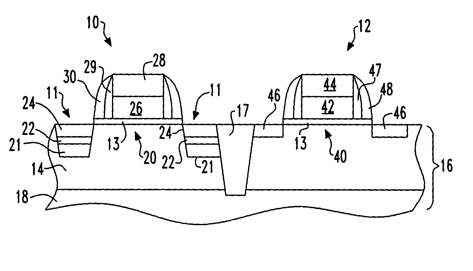
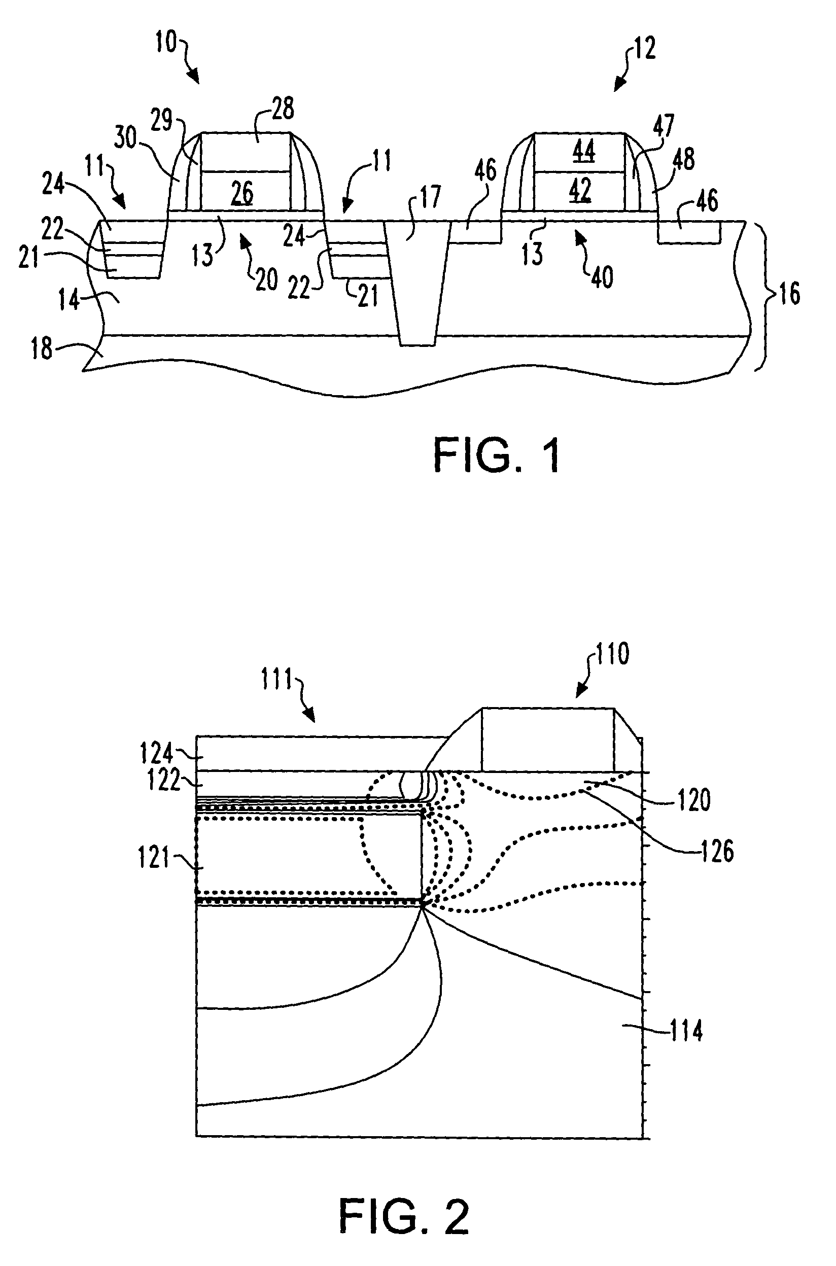
[0019]FIG. 1 illustrates a p-type field effect transistor (PFET) and an n-type field effect transistor (NFET) according to an embodiment of the invention. As illustrated in FIG. 1, the PFET 10 and NFET 12 are fabricated in a single-crystal semiconductor region 14 of a substrate 16, separated by a trench isolation region 17, typically of oxide. The substrate 16 may either be a bulk substrate or may preferably be a semiconductor-on-insulator or silicon-on-insulator (SOI) substrate in which a relatively thin layer of a semi-conductor is formed over an insulating layer 18. When field effect transistors (FETs) are formed in such SOI substrates, faster switching operation is often achieved than otherwise, because junction capacitance between the channel region of the transistor and the bulk substrate is eliminated. The substrate is preferably a bulk single-crystal silicon substrate, and more preferably a silicon SOI substrate having a single-crystal silicon region above an insulating laye...


PUM


Abstract

A p-type field effect transistor (PFET) and an n-type field effect transistor (NFET) of an integrated circuit are provided. A first strain is applied to the channel region of the PFET but not the NFET via a lattice-mismatched semiconductor layer such as silicon germanium disposed in source and drain regions of only the PFET and not of the NFET. A process of making the PFET and NFET is provided. Trenches are etched in the areas to become the source and drain regions of the PFET and a lattice-mismatched silicon germanium layer is grown epitaxially therein to apply a strain to the channel region of the PFET adjacent thereto. A layer of silicon can be grown over the silicon germanium layer and a salicide formed from the layer of silicon to provide low-resistance source and drain regions.

Description

BACKGROUND OF INVENTION [0001] The present invention relates to the fabrication of semiconductor integrated circuits, and more specifically to an apparatus and method of making strained semiconductor complementary metal oxide semiconductor (CMOS) transistors having lattice-mismatched source and drain regions. [0002] Both theoretical and empirical studies have demonstrated that carrier mobility with a transistor is greatly increased when a strain is applied to the transistor's conduction channel. In p-type field effect transistors, the application of a compressive longitudinal strain to the conduction channel is known to increase the drive currents of the PFET. However, if that same strain is applied to the conduction channel of an NFET, its performance decreases. [0003] It has been proposed to apply a tensile longitudinal strain to the conduction channel of an NFET and apply a compressive longitudinal strain to the conduction channel of a PFET. Such proposals have focused on masked ...

Claims


Application Information

Patent Timeline
IPC IPC(8): H01L21/20H01L21/336H01L21/8238H01L21/84H01L27/092H01L27/12
CPCH01L21/02532H01L21/02636H01L21/823807H01L21/823814H01L21/84H01L29/7848H01L27/1203H01L29/165H01L29/6656H01L29/66628H01L29/66636H01L27/0922H01L21/8238
Inventor CHEN, HUAJIECHIDAMBARRAO, DURESETIGLUSCHENKOV, OLEG G.STEEGEN, AN L.YANG, HAINING S.
Owner SEMICON MFG INT (SHANGHAI) CORP
Why Eureka
Try Eureka