Electron emitter device for data storage applications and method of manufacture

a data storage and emitter technology, applied in the manufacture of electrode systems, electric discharge tubes/lamps, instruments, etc., can solve the problems of high-vacuum, high cost, and difficult to achieve high-vacuum, so as to optimize the operation ability of tip-based emitters and enhance the ability of flat emitter structures

Inactive Publication Date: 2005-02-10
HEWLETT PACKARD DEV CO LP
View PDF7 Cites 26 Cited by
  • Summary
  • Abstract
  • Description
  • Claims
  • Application Information

AI Technical Summary

Benefits of technology

[0009] The field emission device further includes a focusing electrode that is electrically coupled to a solid state field controlled emitter and operates in conjunction with the extractor electrode to focus the electron beam emission to a small spot size within the range of 10 to 50 nanometers at the storage medium surface. Dielectric insulating layers are placed between the extractor electrode and the emitter electrode and between the extractor electrode and the focusing electrode. The use of the Schottky metal-semiconductor barrier enhances the ability of flat emitter structures to operate in field emission devices and further optimizes the ability of tip-based emitters in their operation.

Problems solved by technology

Further, the manufacturing steps necessary to produce and fabricate field tip emitters is extremely complex.
High-vacuums are expensive and difficult to achieve.

Method used


Image

  • Electron emitter device for data storage applications and method of manufacture
  • Electron emitter device for data storage applications and method of manufacture
  • Electron emitter device for data storage applications and method of manufacture

Examples


Embodiment Construction

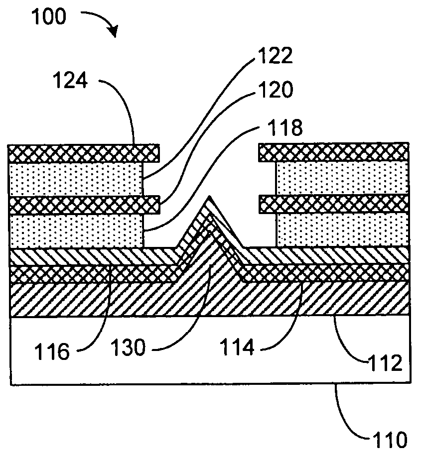
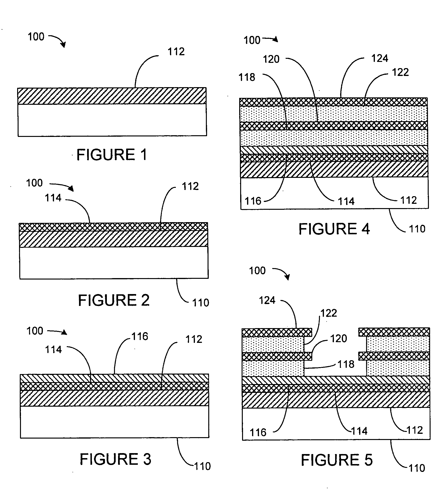
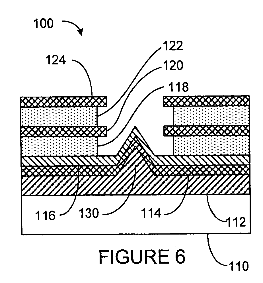
[0020] An improved field emission emitter structure that is typically utilized within an ultra-high density storage device is disclosed in FIGS. 1-6. The emitter structure 100 utilizes a solid state mechanism to enhance and improve electron emission for use in structures such as ultra-high density storage devices, previously disclosed in U.S. Pat. No. 5,557,596, incorporated by reference for all purposes, and in field emission-based display systems such as the type disclosed in U.S. Pat. No. 5,587,628, incorporated by reference for all purposes. The structure is also based on the structure described and illustrated in WO 00 / 70638, published Nov. 23, 2000, as well as French patent No. FR9906254.

[0021] The solid state mechanism utilizes a thin metal layer placed upon the emitter electrode of the field emission electron emitter device. Next, a thin layer of wide band-gap semiconductor material is placed upon the metal layer, which forms a Schottky metal-semiconductor junction to enhan...


PUM

PropertyMeasurementUnit
sizeaaaaaaaaaa
thicknessaaaaaaaaaa
thicknessaaaaaaaaaa

Abstract

A field emission device, which among other things may be used within an ultra-high density storage system, is disclosed. The emitter device includes an emitter electrode, an extractor electrode, and a solid-state field controlled emitter that utilizes a Schottky metal-semiconductor junction or barrier. The Schottky metal-semiconductor barrier is formed on the emitter electrode and electrically couples with the extractor electrode such that when an electric potential is placed between the emitter electrode and the extractor electrode, a field emission of electrons is generated from an exposed surface of the semiconductor layer. Further, the Schottky metal may be selected from typical conducting layers such as platinum, gold, silver, or a conductive semiconductor layer that is able to provide a high electron pool at the barrier. The semiconductor layer placed on the Schottky metal is typically very weakly conductive of n-type and has a wide band gap in order to create conditions conducive to creating induced negative electron affinity at applied fields necessary to provide electron emission. One type of wide band-gap material can be selected from titanium dioxide or titanium nitride or other comparable materials.

Description

BACKGROUND OF THE INVENTION [0001] Another application in emitter devices is described in commonly assigned co-pending U.S. patent application Ser. No. ______ (HP docket number 10004241-1), entitled “PLANAR ELECTRON EMITTER APPARATUS WITH IMPROVED EMISSION AREA AND METHOD OF MANUFACTURE,” the disclosure of which is hereby incorporated herein by reference. [0002] The present invention relates generally to ultra-high density storage devices using field emission electron emitter technology and, more particularly, the present invention relates to an improved field emission emitter that utilizes a Schottky metal-semiconductor barrier to provide solid state emission for use within the storage device. [0003] Memory storage systems have made tremendous advancements over the years from the first use of magnetic tape to magnetic hard drives and now optical drives as well as sophisticated fast memory such as S-RAM and D-RAM. A more recent development has utilized field emission electron emitte...

Claims


Application Information

Patent Timeline
Patent Type & Authority Applications(United States)
IPC IPC(8): G11C11/42G11B9/00H01J1/304H01J1/308H01J9/02
CPCB82Y10/00H01J1/308G11B9/1409G11B9/14
Inventor BIRECKI, HENRYKBINH, VU THIENLAM, SI-TYKUO, HUEI PEINABERHUIS, STEVEN L.
Owner HEWLETT PACKARD DEV CO LP
Why Eureka
Try Eureka