Pattern forming method, pattern forming apparatus, device manufacturing method, conductive film wiring, electro-optical device, and electronic apparatus

a pattern forming and pattern technology, applied in the direction of solid-state devices, metal-layer products, metallic material coating processes, etc., can solve the problems of lack of uniform appearance between the wiring patterns, and achieve excellent electrical characteristic and display properties, without lack of uniform appearance

Inactive Publication Date: 2005-02-10
SEIKO EPSON CORP
View PDF5 Cites 101 Cited by
  • Summary
  • Abstract
  • Description
  • Claims
  • Application Information

AI Technical Summary

Benefits of technology

[0033] According to the present invention, it is possible to provide conductive film wiring without the lack of uniformity in appearance.
[0034] The present invention also provides an electro-optical device comprising the aforementioned conductive film wiring. In addition, the present invention also provides an electronic apparatus comprises the aforementioned electro-optical device. According to the present invention, since the conductive film pattern having a uniform line width and not having the lack of uniformity in appearance is provided, it is possible to obtain excellent electrical characteristic and display property.

Problems solved by technology

On the other hand, when a plurality of wiring patterns are formed by arranging a plurality of droplets on a substrate, arrangement of the droplets may be different for each wiring pattern, so that there is a problem that a lack of uniformity in appearance between the wiring patterns occurs.

Method used


Image

  • Pattern forming method, pattern forming apparatus, device manufacturing method, conductive film wiring, electro-optical device, and electronic apparatus
  • Pattern forming method, pattern forming apparatus, device manufacturing method, conductive film wiring, electro-optical device, and electronic apparatus
  • Pattern forming method, pattern forming apparatus, device manufacturing method, conductive film wiring, electro-optical device, and electronic apparatus

Examples


Embodiment Construction

[0055] Pattern Forming Method

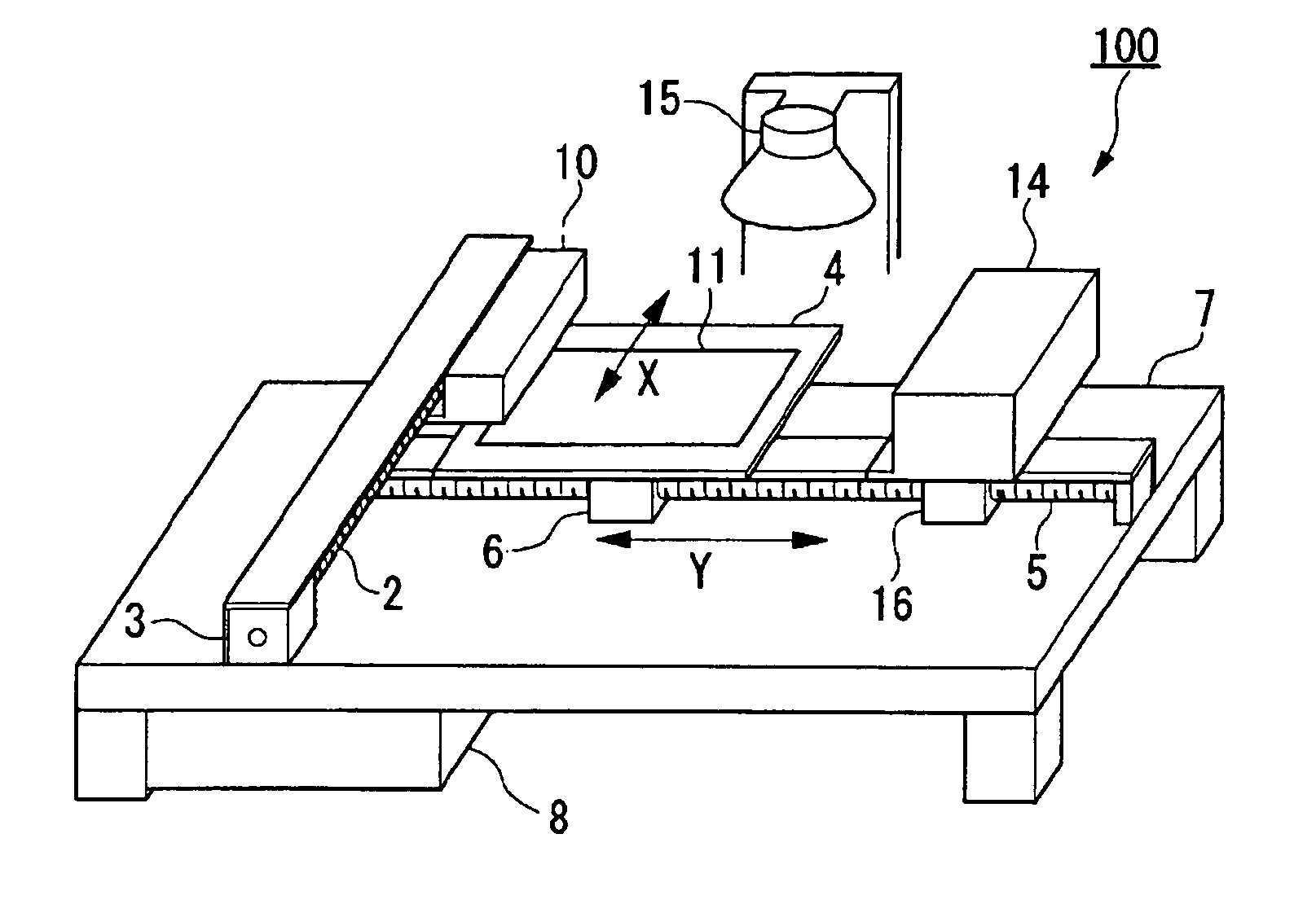
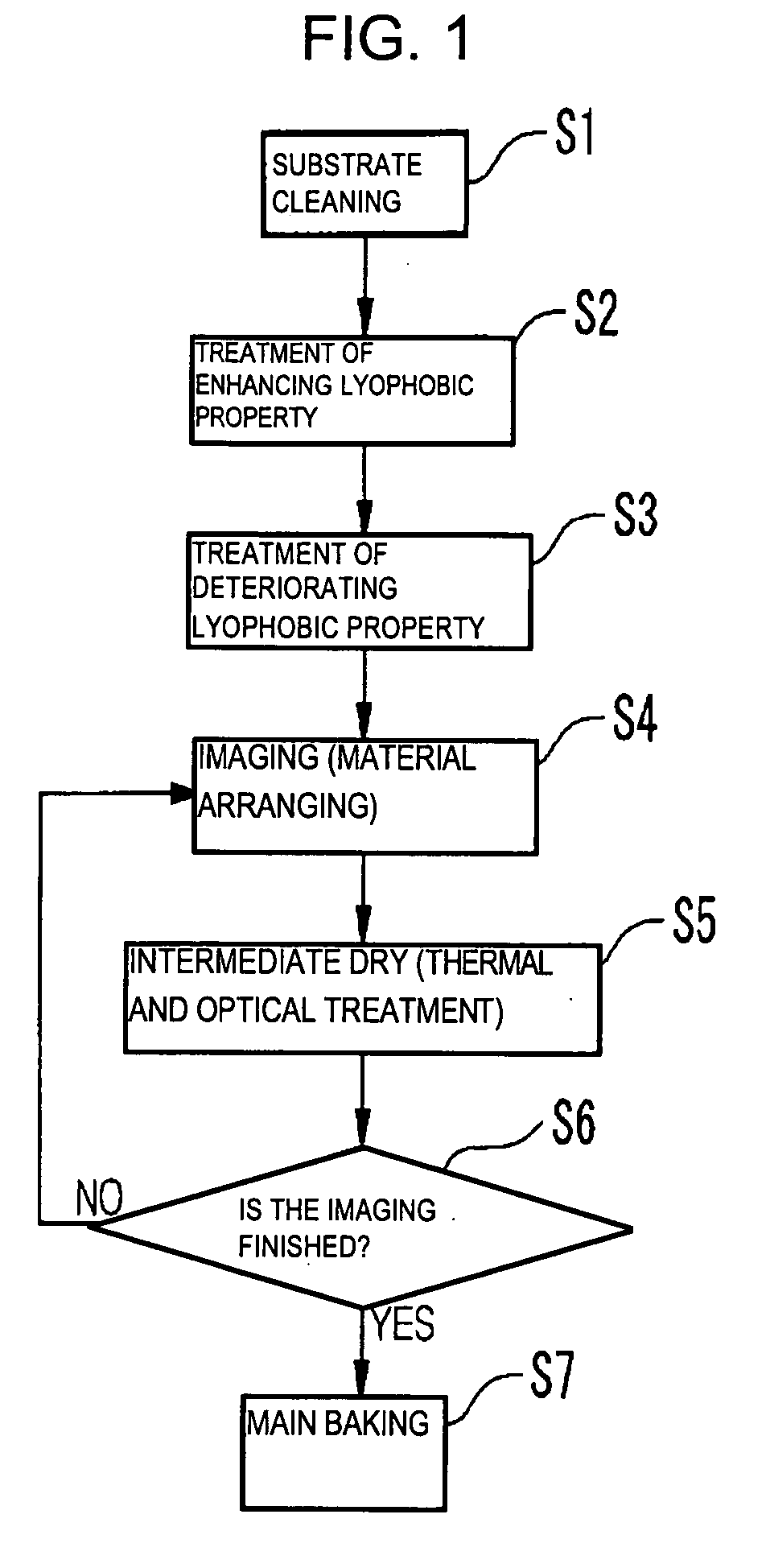
[0056] Hereinafter, a pattern forming method according to the present invention will be described with reference to the accompanying drawings. FIG. 1 is a flowchart of a pattern forming method according to an embodiment of the present invention.

[0057] Here, in the present embodiment, a case where a conductive film wiring pattern is formed on a substrate will be described.

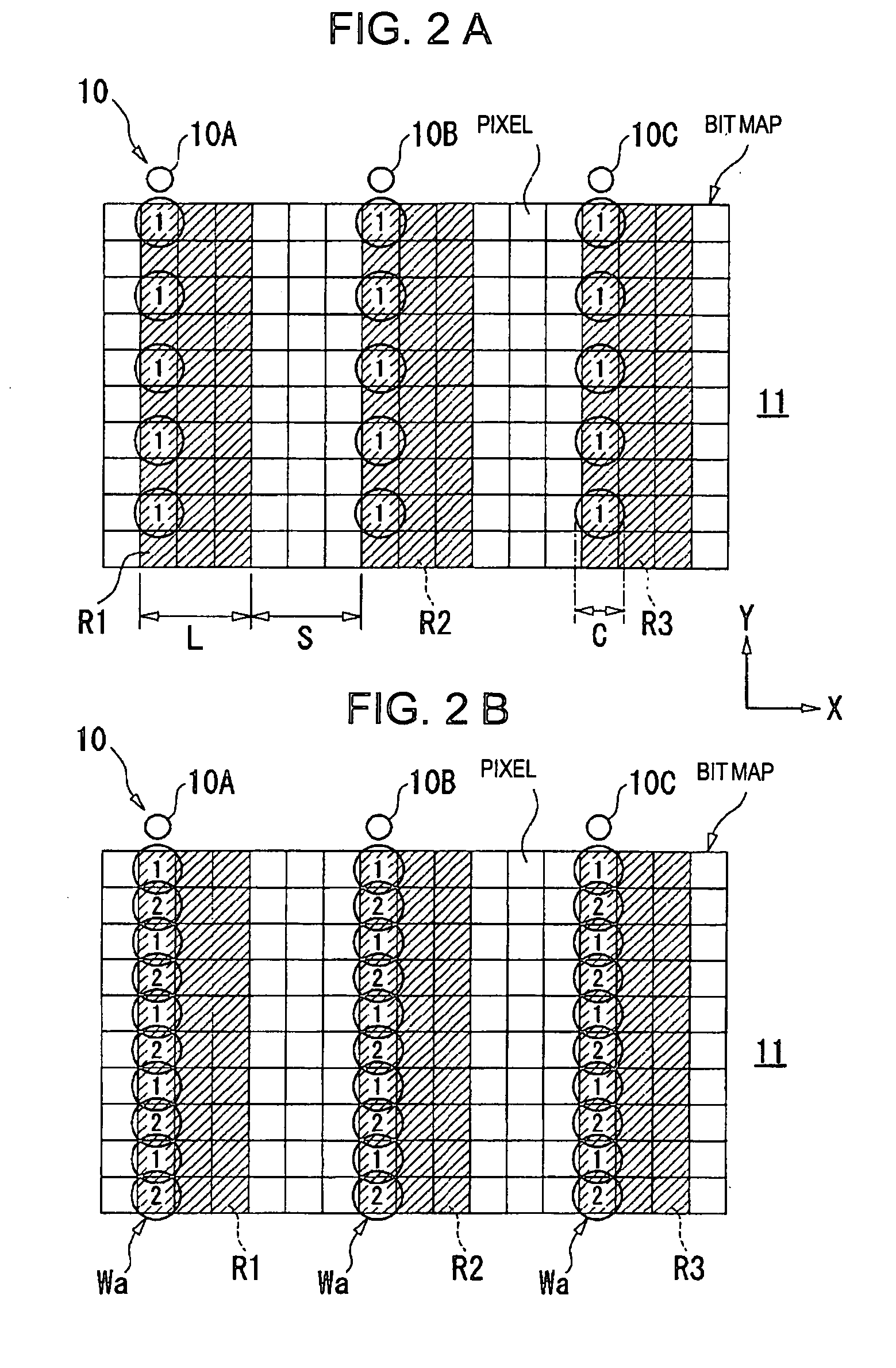
[0058] In FIG. 1, the pattern forming method according to the present embodiment comprises a step (step S1) of cleaning a substrate on which droplets of a liquid material are arranged, using a predetermined solvent; a step (step S2) of performing lyophobic treatment that constitutes a part of a surface treatment step of the substrate; a step (step S3) of performing lyophobic property controlling treatment that constitutes a part of the surface treatment step of adjusting a lyophobic property of the surface of the substrate on which lyophobic treatment is performed; a material arrangem...


PUM

PropertyMeasurementUnit
areaaaaaaaaaaa
diameteraaaaaaaaaa
diameteraaaaaaaaaa

Abstract

A pattern forming method is provided for forming film patterns W1 to W3 by arranging droplets of a liquid material on a substrate. The method comprises the steps of: defining a plurality of pattern forming areas R1 to R3 in which the film patterns should be formed on the substrate; and sequentially arranging a plurality of droplets in the plurality of defined pattern forming areas R1 to R3, thereby forming the film patterns W1 to W3, wherein the droplets are sequentially arranged by setting an arrangement order of the droplets to be substantially equal for the plurality of pattern forming areas R1 to R3.

Description

RELATED APPLICATIONS [0001] This application claims priority to Japanese Patent Application Nos. 2003-088803 filed Mar. 27, 2003 and 2004-031045 filed Feb. 6, 2004 which are hereby expressly incorporated by reference herein in their entireties. BACKGROUND [0002] 1. Technical Field of the Invention [0003] The present invention relates to a pattern forming method and a pattern forming apparatus for forming a film pattern by arranging droplets of a liquid material on a substrate, a method of manufacturing a device, conductive film wiring, an electro-optical device, and an electronic apparatus. [0004] 2. Description of the Related Art [0005] Photolithographic methods have been widely used in methods of manufacturing devices having a fine wiring pattern (film pattern), such as a semiconductor integrated circuit (IC). However, a lot of attention has been paid to a method of manufacturing a device using a droplet discharge method. The droplet discharge method has an advantage in that the c...

Claims


Application Information

Patent Timeline
Patent Type & Authority Applications(United States)
IPC IPC(8): B05C5/00B05D1/26B05D7/00B05D5/12H01L21/288H01L21/3205H01L29/786H01L51/40H05K3/00H05K3/10H05K3/12
CPCH01L21/288Y10T428/24917H05K3/125H01L51/0004H10K71/13H05K3/00B05D5/12
Inventor HIRAI, TOSHIMITSU
Owner SEIKO EPSON CORP
Why Eureka
Try Eureka